Vertical trench IGBT and method for manufacturing the same

一种制造方法、沟槽的技术,应用在半导体/固态器件制造、电气元件、电路等方向,能够解决漏电流变大、缺陷增加、RBSOA耐受性劣化等问题,达到提高耐受性的效果

Active Publication Date: 2013-09-18
MITSUBISHI ELECTRIC CORP
View PDF8 Cites 3 Cited by
  • Summary
  • Abstract
  • Description
  • Claims
  • Application Information

AI Technical Summary

Problems solved by technology

In addition, stress is concentrated at the bottom of the contact plug, whereby defects increase in the Si substrate and leakage current becomes large
As a result, there is a problem of deterioration of RBSOA tolerance

Method used


Image

  • Vertical trench IGBT and method for manufacturing the same
  • Vertical trench IGBT and method for manufacturing the same
  • Vertical trench IGBT and method for manufacturing the same

Examples


Embodiment approach 1

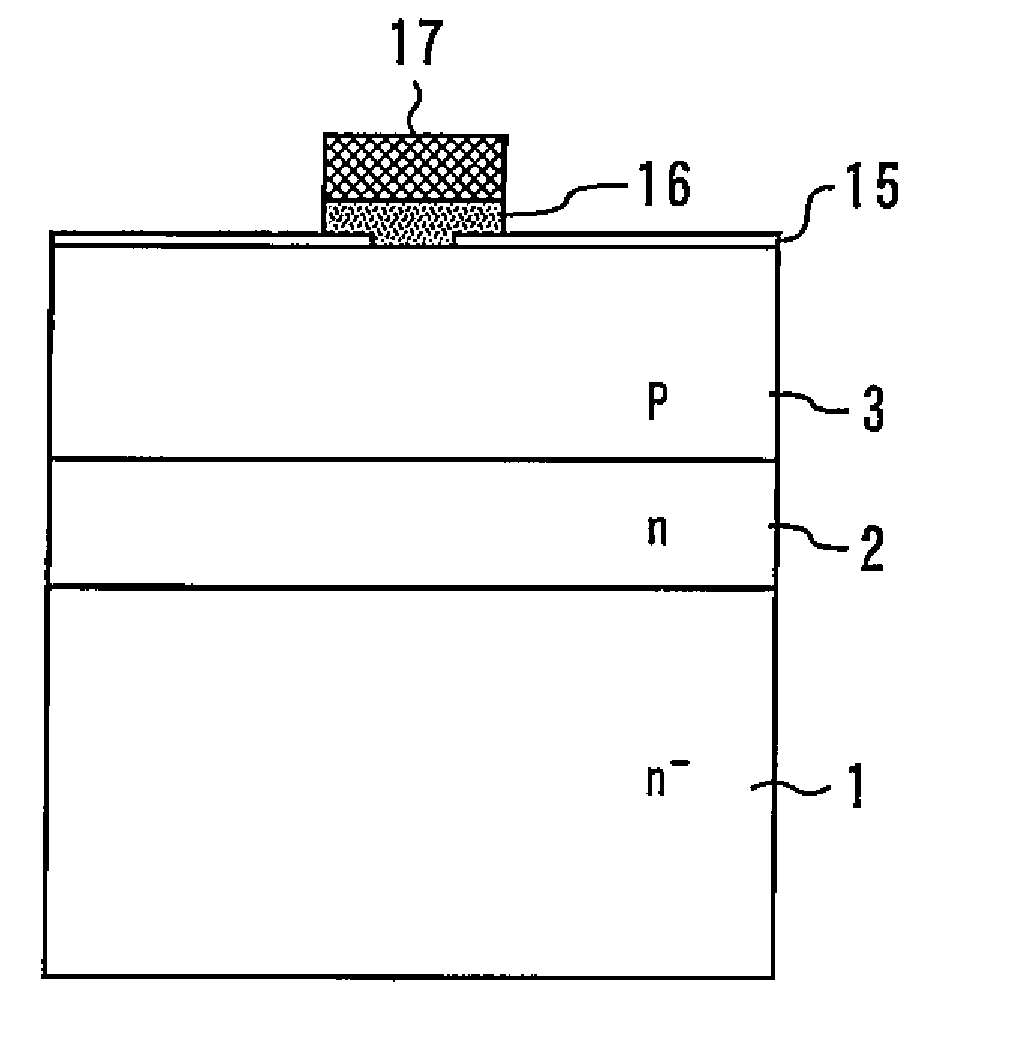
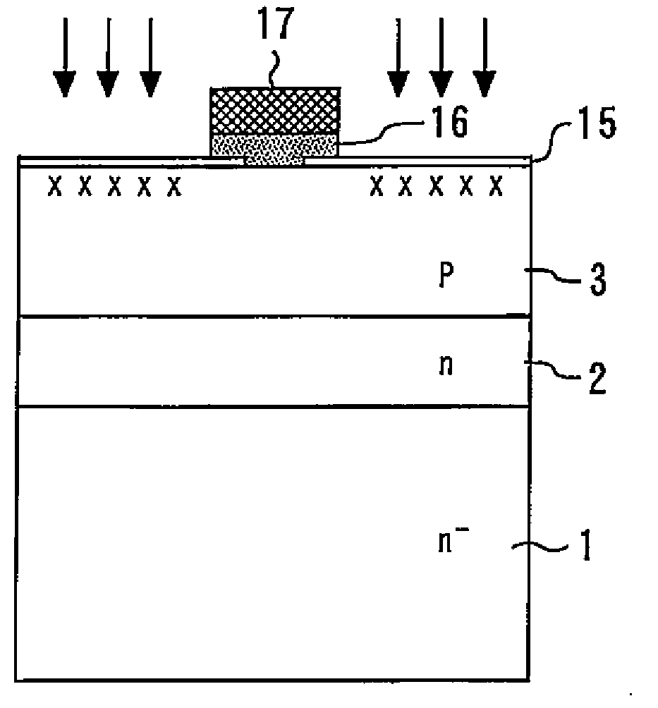
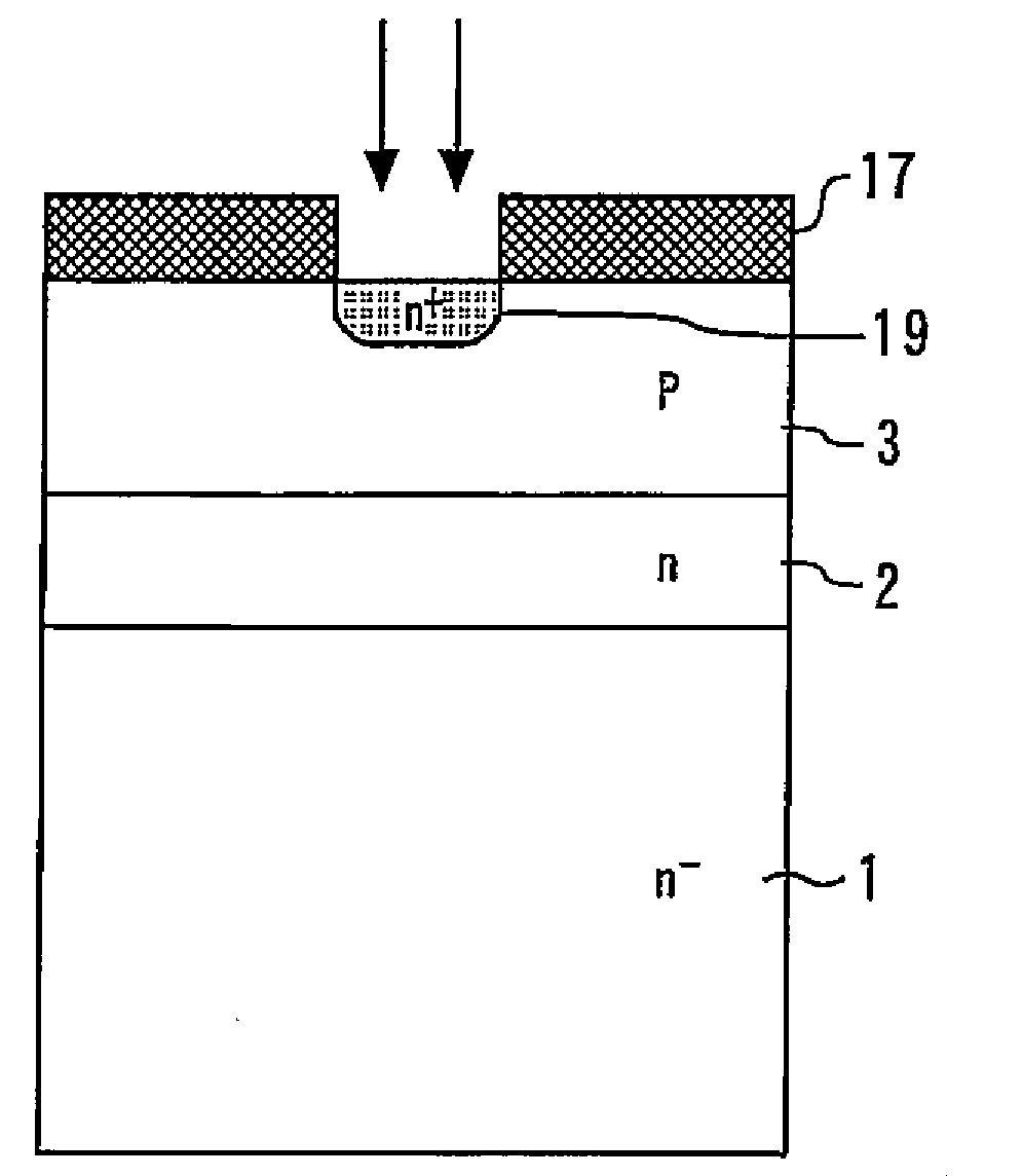
[0032] figure 1 is a perspective view showing the vertical trench IGBT according to Embodiment 1 of the present invention, figure 2 is along figure 1 Cross section of A-A'. in n - An n-type charge storage layer 2 and a p-type body layer 3 are sequentially disposed on an n-type Si substrate 1 . A trench gate 4 is provided in a trench penetrating the p-type body layer 3 via a gate insulating film 5 . Trench gates 4 are arranged in stripes in plan view.

[0033] An n-type emitter layer 6 and a p+-type diffusion layer 8 are provided on the p-type body layer 3 . In plan view, n-type emitter layers 6 and p+-type diffusion layers 8 are alternately arranged between adjacent trench gates 4 in the longitudinal direction of trench gates 4 .

[0034] Interlayer insulating film 9 covers trench gate 4 . Emitter electrode 10 is provided on interlayer insulating film 9 . Contact plug 11 penetrates interlayer insulating film 9 and connects p-type body layer 3 and n-type emitter layer ...

Embodiment approach 2

[0046] Figure 14 It is a perspective view showing a vertical trench IGBT according to Embodiment 2 of the present invention. Figure 15 is along Figure 14 Cross section of A-A'. A polysilicon film 20 having a film thickness of 500 Å to 5000 Å is provided between the p-type body layer 3 , the n-type emitter layer 6 , and the contact plug 11 .

[0047] The polysilicon film 20 can reduce the stress caused by the trench gate 4 and the contact plug 11 in the microcell. Accordingly, it is possible to suppress the increase of defects in the Si substrate. As a result, the junction leakage current is reduced, so that the RBSOA tolerance can be improved.

[0048] In Embodiments 1 and 2, it is preferable to form polysilicon films 16 and 20 simultaneously with polysilicon forming trench gate 4 , polysilicon forming polysilicon electrode 21 of a poly-poly capacitor, polysilicon resistor 22 , and the like. Thereby, the number of steps can be reduced.

[0049] In addition, the vertic...


PUM


Abstract

A method for manufacturing a vertical trench IGBT includes: forming a body layer of a second conductivity type on a semiconductor substrate of a first conductivity type; forming a trench passing through the body layer; forming a trench gate in the trench via a gate insulating film; forming a polysilicon film containing an impurity of a first conductivity type on the body layer; diffusing the impurity from the polysilicon film into the body layer to form an emitter layer of a first conductivity type on the body layer; and forming a collector layer of a second conductivity type on a lower surface of the semiconductor substrate.

Description

technical field [0001] The present invention relates to a vertical trench IGBT (Insulated Gate Bipolar Transistor: insulated gate bipolar transistor) and a manufacturing method thereof. Background technique [0002] Conventionally, the emitter layer of the vertical trench IGBT is formed by impurity implantation and heat treatment. In addition, in order to miniaturize the cell structure of the vertical trench IGBT, it is necessary to make a plug in the contact structure, but the contact plug is in contact with the semiconductor layer through a thin barrier metal. [0003] In addition, it has been proposed to form a diffusion layer by diffusion of impurities derived from polysilicon or to provide a polysilicon film between a semiconductor layer and a contact plug in a lateral transistor (for example, refer to Patent Documents 1 to 3). [0004] prior art literature [0005] patent documents [0006] Patent Document 1: Japanese Patent Application Laid-Open No. 8-97226; [00...

Claims


Application Information

Patent Timeline
Patent Type & Authority Applications(China)
IPC IPC(8): H01L21/331H01L29/08H01L29/06H01L29/739
CPCH01L29/66348H01L29/7397H01L29/0696H01L29/0839H01L21/18H01L29/739
Inventor 藤井秀纪
Owner MITSUBISHI ELECTRIC CORP
Why Eureka
Try Eureka