Thin film photoconductive detector and manufacturing method and application thereof

A detector and photoconductive technology, applied in semiconductor/solid-state device manufacturing, photovoltaic power generation, electric solid-state devices, etc., can solve the problems of poor performance of one-dimensional nano-devices, achieve high responsivity, simple preparation method, and improve responsivity Effect

Active Publication Date: 2015-07-15
INST OF CHEM CHINESE ACAD OF SCI
View PDF6 Cites 1 Cited by
  • Summary
  • Abstract
  • Description
  • Claims
  • Application Information

AI Technical Summary

Problems solved by technology

Using the quantum surface effect and size effect of quantum dots will make inorganic materials absorb more light. Optoelectronic devices based on quantum dots can exhibit large R and G values, but their performance is much worse than that of one-dimensional nanodevices.

Method used


Image

  • Thin film photoconductive detector and manufacturing method and application thereof
  • Thin film photoconductive detector and manufacturing method and application thereof
  • Thin film photoconductive detector and manufacturing method and application thereof

Examples


Embodiment 1

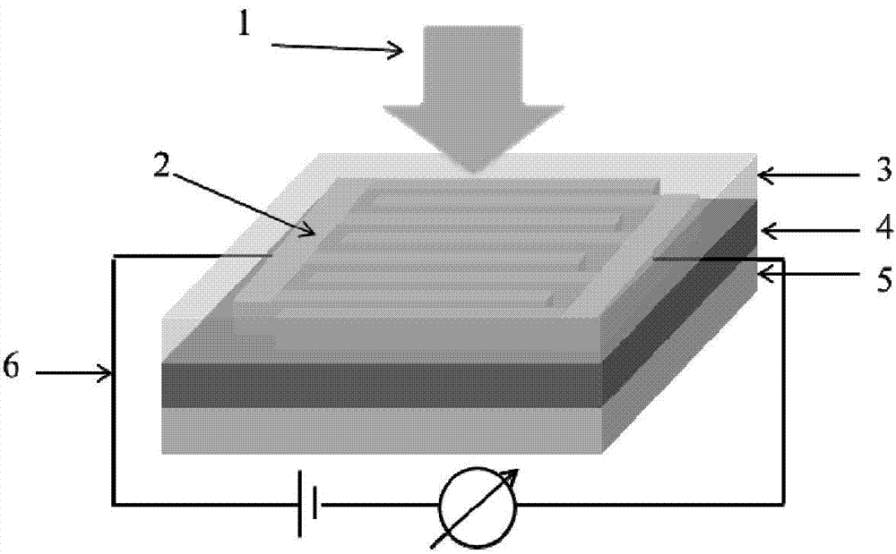
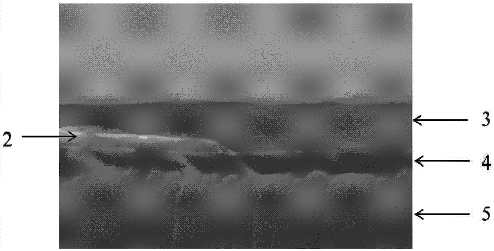
[0055] 1) if figure 1 As shown, zinc acetate was dissolved in methoxyethanol to obtain a solution with a concentration of 40mg / ml, spin-coated at 1000rpm for 60s on a glass substrate 5 with a thickness of 3mm and annealed at 500°C for 1h to obtain a carrier transport layer 4 with a thickness of 50nm .

[0056] The material constituting the carrier transport layer is zinc oxide;

[0057] 2) On the carrier transport layer obtained in step 1), the positive electrode layer 2 and the negative electrode layer 2 were respectively vacuum evaporated, the length of the positive electrode and the negative electrode was 8800 μm, the distance between the two electrodes was 80 μm, and the vacuum degree during vacuum evaporation was 1 ×10 -4 Pa.

[0058] Both the positive electrode layer and the negative electrode layer are made of aluminum;

[0059] The thickness is 50nm;

[0060] 3) Prepare a layer of light-absorbing layer by spin coating on the positive electrode layer and the negat...

Embodiment 2

[0071] According to the steps of embodiment 1, only step 3) is replaced by the following steps:

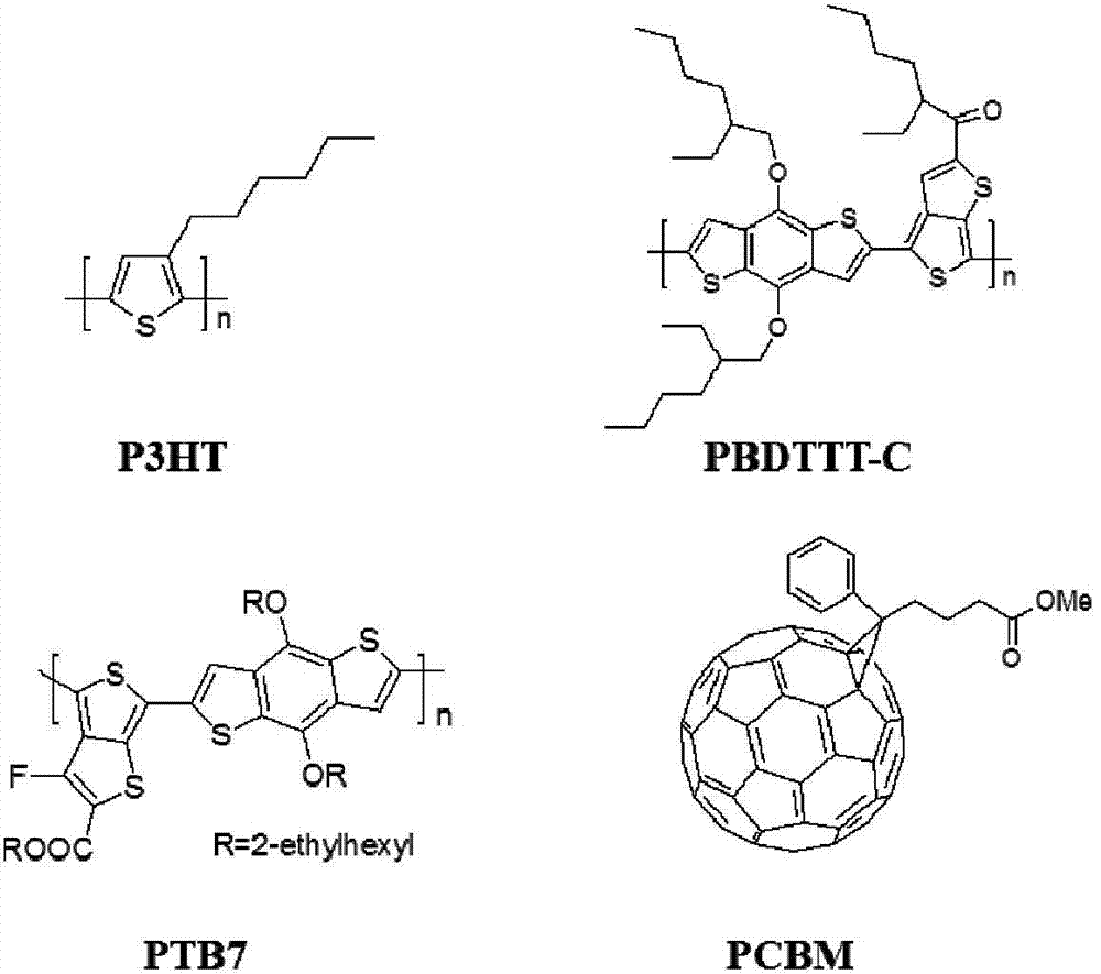
[0072] 3) Prepare a light-absorbing layer by spin coating on the positive electrode layer and the negative electrode layer obtained in step 2). The specific steps include: adding PBDTTT-C with a relative molecular mass of 60000g / mol and PCBM with a relative molecular mass of 910.88g / mol by weight After mixing evenly at a ratio of 1:1.5, it was dissolved in o-dichlorobenzene to obtain a solution with a concentration of 40 mg / ml. After spin coating at 1000 rpm for 60 seconds, the substrate was annealed at 100° C. for 10 minutes to obtain a light-absorbing layer 3 with a thickness of 150 nm, and obtain the present invention. Thin-film photoconductive detectors;

[0073] According to the same steps as above, only the PBDTTT-C used in step 3) is replaced with PTB7 with a relative molecular mass of 10000-60000 g / mol, and another thin film photoconductive detector provided by the present...


PUM


Abstract

The invention discloses a thin film photoconductive detector and a manufacturing method and application thereof. The thin film photoconductive detector comprises a substrate, a carrier transport layer, an electrode layer and a light absorption layer from bottom to top, wherein the electrode layer consists of an anode layer and a cathode layer positioned on the same layer. The detector integrates high migration ratio of an inorganic material and high light absorptivity of an organic material; when light irradiates onto an organic layer of a photoelectric device, the uppermost organic material layer absorbs light to generate carriers; and by virtue of energy level difference between an inorganic layer and the organic layer and the concentration difference of the carriers, the photo-generated carriers enter the inorganic material layer and can be fast collected by electrodes, thereby having large G and R values. Meanwhile, due to high migration rate of the inorganic material, the light current response time and the fall time of the device are greatly shortened, and therefore the sensitivity of the thin film photoconductive device is improved; and the thin film photoconductive detector has an important application value.

Description

technical field [0001] The invention relates to a thin-film photoconductive detector and its preparation method and application. Background technique [0002] At present, the known photoconductive detector structure is composed of two horizontal electrodes and a photosensitive layer in the middle. Connect the photoconductive device into a loop and add a bias electric field. When the incident light contacts the detector, the photosensitive layer inside the detector generates electron-hole pairs, which are separated under the action of the electric field and collected by the electrodes. Photocurrent is formed, and the intensity and size of light can be characterized by the intensity of photocurrent, which can be used for light detection, image imaging or biosensing and other directions. Therefore, the sensitivity of the device to light is very important. Usually we use two important parameters to characterize such a sensitivity: responsivity R and photoelectric gain G. R rep...

Claims


Application Information

Patent Timeline
Patent Type & Authority Patents(China)
IPC IPC(8): H01L51/46H01L51/48
CPCY02E10/549
Inventor 靳志文王吉政张志国
Owner INST OF CHEM CHINESE ACAD OF SCI
Why Eureka
Try Eureka