Preparation method of Si nanowire arrays
A nanowire array and reaction solution technology, applied in the field of preparation of Si nanowire arrays, can solve the problem that semiconductor materials cannot be mass-produced in industry, and achieve the effects of low equipment requirements, simple preparation, and good controllability.
- Summary
- Abstract
- Description
- Claims
- Application Information
AI Technical Summary
Problems solved by technology
Method used
Image

Examples
Embodiment 1
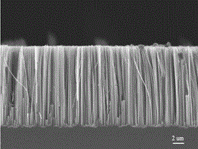
[0020] 1) After cleaning the heavily doped (1 0 0) silicon wafer with a resistivity of 0.001~0.01 Ω cm by RCA method, put sulfuric acid with a mass concentration of 97% and hydrogen peroxide with a mass concentration of 30% in a volume ratio of 3:1 Soak in the mixture for 10 min. Then rinse with deionized water, and soak in 10% hydrofluoric acid buffer solution for 3 min.
[0021] 2) Mix hydrofluoric acid and silver nitrate to prepare reaction solution I, the concentration of hydrofluoric acid is 4.65 mol / L, and the concentration of silver nitrate is 0.02 mol / L; mix hydrofluoric acid and hydrogen peroxide to prepare reaction solution II, the concentration of hydrofluoric acid is 4.65 mol / L, and the concentration of hydrogen peroxide is 0.5 mol / L;
[0022] 3) Put the polished side of the silicon wafer treated in step 1) into the reaction solution I horizontally, take it out after soaking for 1 min, rinse it with deionized water, put it into the reaction solution II, react for ...
Embodiment 2
[0025] 1) After cleaning the heavily doped (1 0 0) silicon wafer with a resistivity of 0.001~0.01 Ω cm by RCA method, put sulfuric acid with a mass concentration of 97% and hydrogen peroxide with a mass concentration of 30% in a volume ratio of 3:1 Soak in the mixture for 10 min. Then the wafers were rinsed with deionized water, and soaked in 10% hydrofluoric acid buffer solution for 3 min.
[0026] 2) Mix hydrofluoric acid and silver nitrate to prepare reaction solution I, the concentration of hydrofluoric acid is 4.65 mol / L, and the concentration of silver nitrate is 0.02 mol / L; mix hydrofluoric acid and hydrogen peroxide to prepare reaction solution II, the concentration of hydrofluoric acid is 4.65 mol / L, and the concentration of hydrogen peroxide is 0.5 mol / L;
[0027] 3) Put the polished side of the silicon wafer treated in step 1) into the reaction solution I horizontally, soak for 1 min, take it out, rinse it with deionized water, put it into the reaction solution II,...
Embodiment 3
[0030] 1) After cleaning the heavily doped (1 0 0) silicon wafer with a resistivity of 0.001~0.01 Ω cm by RCA method, put sulfuric acid with a mass concentration of 97% and hydrogen peroxide with a mass concentration of 30% in a volume ratio of 3:1 Soak in the mixture for 10 min. Then rinse with deionized water, and soak in 10% hydrofluoric acid buffer solution for 3 min.
[0031] 2) Mix hydrofluoric acid and silver nitrate to prepare reaction solution I, the concentration of hydrofluoric acid is 4.65 mol / L, and the concentration of silver nitrate is 0.02 mol / L; mix hydrofluoric acid and hydrogen peroxide to prepare reaction solution II, the concentration of hydrofluoric acid is 4.65 mol / L, and the concentration of hydrogen peroxide is 0.5 mol / L;
[0032] 3) Put the polished side of the silicon wafer treated in step 1) into the reaction solution I horizontally, take it out after soaking for 1 min, rinse it with deionized water, put it into the reaction solution II, react for ...
PUM
 Abstract
Description
Claims
Application Information
 - R&D Engineer
- R&D Manager
- IP Professional
- Industry Leading Data Capabilities
- Powerful AI technology
- Patent DNA Extraction
Browse by: Latest US Patents, China's latest patents, Technical Efficacy Thesaurus, Application Domain, Technology Topic.
© 2024 PatSnap. All rights reserved.Legal|Privacy policy|Modern Slavery Act Transparency Statement|Sitemap