JFET and MESFET structures for low voltage high current and high frequency applications

a high-current, high-current technology, applied in the direction of basic electric elements, semiconductor devices, electrical equipment, etc., can solve the problems of high transient current load, large power consumption in the rectifying process, and difficult challenges in the semiconductor industry, so as to reduce junction capacitance, accurate control, and gate length can be very tightly controlled

Inactive Publication Date: 2006-05-16
POWER INTEGRATIONS INC
View PDF4 Cites 51 Cited by
  • Summary
  • Abstract
  • Description
  • Claims
  • Application Information

AI Technical Summary

Benefits of technology

[0011]Accordingly, embodiments of the present invention are directed to JFETS and MESFETS suitable for low voltage, high current and high frequency applications. Embodiments of the present invention include transistor structures that comprise an oxide layer disposed under the gate region to reduce junction capacitance. Gate length can be very tightly controlled by according to the present invention by partially removing the bottom oxide layer and exposing windows into the substrate. Therefore, Vt can be very accurately controlled according the present invention. For normally off transistor structures, the gate current is reduced at Vg in forward bias. Moreover, silicide is used in the gate structure to further reduce gate resistance. According to the present invention, a very thin gate can be realized, under 1000 angstroms, by dipping of the spacer oxide to allow high frequency applications. Embodiments of the present invention provide the above advantages and others not specifically mentioned above but described in the sections to follow.
[0012]Embodiments of the present invention are directed to JFET and MESFET structures (transistor structures), and processes of making same, for low voltage, high channel current and high frequency applications. The structures may be used in normally-on (e.g., depletion mode) or normally-off modes. The structures include an oxide layer positioned under the gate region which effectively reduces the junction capacitance (gate to drain) of the structures. For normally off modes, the transistor structures reduce gate current at Vg in forward bias. In one embodiment, a silicide is positioned in part of the gate to reduce gate resistance. The structures are also characterized in that they have a thin gate due to the dipping of the spacer oxide, which can be below 1000 angstroms. This feature results in fast switching speeds for high frequency applications.

Problems solved by technology

The semiconductor industry faces difficult challenges in satisfying the expanding needs to provide transistors that are suitable for power management with low voltage applications, e.g., below 3 volts.
However, the transient current loads can be very high.
Unfortunately, most of the power is consumed in the rectifying process.
Therefore, power supply systems built with such types of p-n junctions are not really suitable for low voltage applications.
Even the Schottky barrier diodes with a forward voltage drop below 0.5 volts are not a suitable solution to provide rectifiers or power switching devices for operation under the low voltage conditions.
However, such naturally off JFET transistors are not very useful in conventional configurations due to the longer current channel thus limiting the current capacity with a high on-resistance.
The long current channel and high-on resistance limit the usefulness of JFET transistors particularly the high on-resistance prevents such transistors for use in applications in modern electronic devices operated with extremely low voltages.
A problem with this conventional JFET structure 10 is that it has a very long channel length thereby creating a large channel resistance.
Further, gate diffusion is very difficult to control in the JFET structure 10 meaning that the threshold voltage, Vt, is difficult to control.
The on-resistance would not be adequate for extremely-low voltage applications required by modern electronic devices as discussed above.
The normally-on JFET transistors disclosed in this patent are operated with high voltage and therefore they are not suitable to satisfy the requirements of modern portable electronic devices that require extremely low voltage and relatively high current capacity.
The JFET transistors disclosed in this patent are not suitable for low voltage and high current applications.

Method used


Image

  • JFET and MESFET structures for low voltage high current and high frequency applications
  • JFET and MESFET structures for low voltage high current and high frequency applications
  • JFET and MESFET structures for low voltage high current and high frequency applications

Examples


Embodiment Construction

[0039]In the following detailed description of the present invention, transistor structures (JFET and MESFET) for low voltage, high current and high frequency applications, numerous specific details are set forth in order to provide a thorough understanding of the present invention. However, it will be recognized by one skilled in the art that the present invention may be practiced without these specific details or with equivalents thereof. In other instances, well known methods, procedures, components, and circuits have not been described in detail as not to unnecessarily obscure aspects of the present invention.

[0040]U.S. Pat. No. 6,251,716, entitled “JFET Structure and Manufacture Method for Low On-Resistance and Low Voltage Application,” issued Jun. 26, 2001, and assigned to the assignee of the present invention, is hereby incorporated herein by reference.

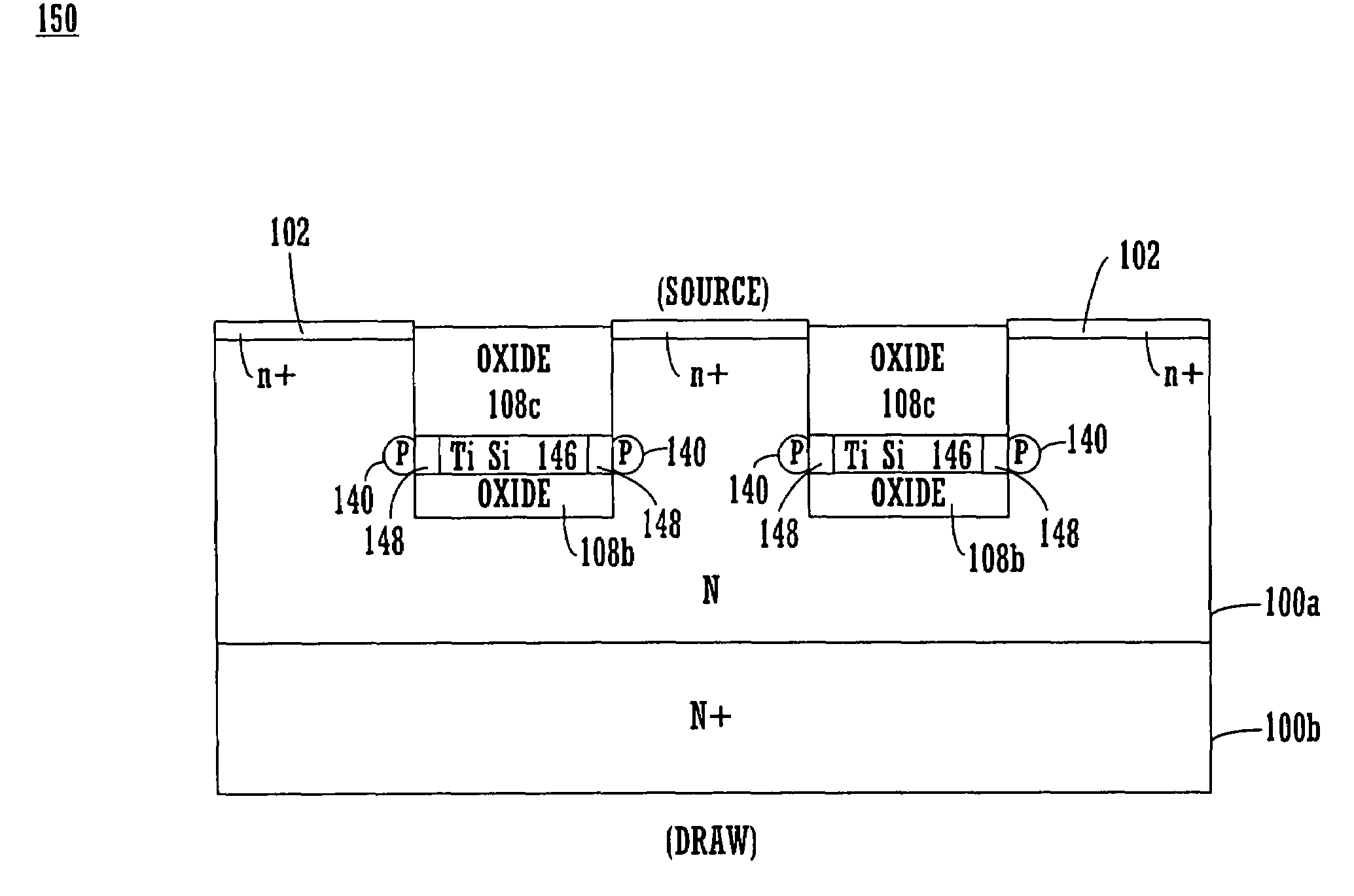
Novel JFET Device and Formation Thereof

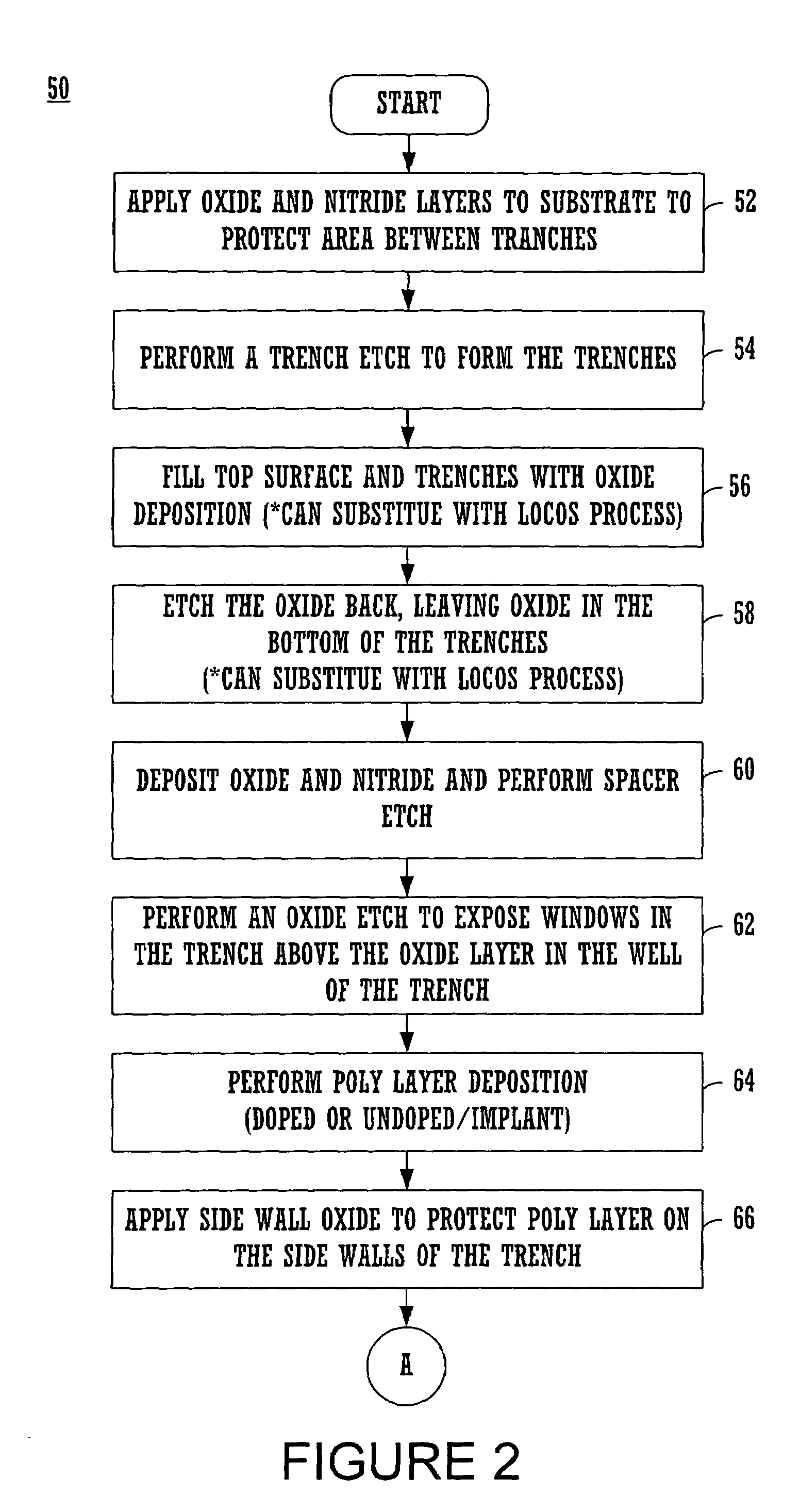
[0041]FIGS. 2–3 illustrate a flow diagram of steps 50 used in accordance with an embod...


PUM


Abstract

JFET and MESFET structures, and processes of making same, for low voltage, high current and high frequency applications. The structures may be used in normally-on (e.g., depletion mode) or normally-off modes. The structures include an oxide layer positioned under the gate region which effectively reduces the junction capacitance (gate to drain) of the structure. For normally off modes, the structures reduce gate current at Vg in forward bias. In one embodiment, a silicide is positioned in part of the gate to reduce gate resistance. The structures are also characterized in that they have a thin gate due to the dipping of the spacer oxide, which can be below 1000 angstroms and this results in fast switching speeds for high frequency applications.

Description

[0001]This patent application is a Divisional of patent application Ser. No. 10 / 153,012, filed on May 20, 2002 and now U.S. Pat. No. 6,921,932 B1, entitled “JFET AND MESFET STRUCTURES FOR LOW VOLTAGE, HIGH CURRENT AND HIGH FREQUENCY APPLICATIONS”, by Yu et al., which is incorporated herein by reference in its entirety.BACKGROUND OF THE INVENTION[0002]1. Field of the Invention[0003]The present invention relates to the field of semiconductor devices. More specifically, the field of the present invention is directed to junction field effect transistors (JFETS) and MESFETS for use in low voltage, high frequency and high current applications.[0004]2. Related Art[0005]The semiconductor industry faces difficult challenges in satisfying the expanding needs to provide transistors that are suitable for power management with low voltage applications, e.g., below 3 volts. As the feature size of the integrated circuits (ICs) become ever smaller and electronic devices are continuously being minia...

Claims


Application Information

Patent Timeline
Patent Type & Authority Patents(United States)
IPC IPC(8): H01L21/335H01L21/337H01L21/338H01L29/772H01L29/808H01L29/812
CPCH01L29/66848H01L29/66909H01L29/8122H01L29/8083H01L29/7722
Inventor YU, HO-YUANLIVA, VALENTINO L.
Owner POWER INTEGRATIONS INC
Why Eureka
Try Eureka