
Non-destructive power MOS tube single-event burnout effect detecting circuit and non-destructive power MOS tube single-event burnout effect detecting method

A single-particle burning, MOS tube technology, applied in the direction of single semiconductor device testing, etc., can solve the problems that cannot be repeated many times, cannot determine the threshold value of the gate control voltage and drain voltage of the MOS tube, etc., and achieves simple operation. Effect

Active Publication Date: 2013-10-09
CHINA ACADEMY OF SPACE TECHNOLOGY
View PDF3 Cites 8 Cited by
  • Summary
  • Abstract
  • Description
  • Claims
  • Application Information

AI Technical Summary

Problems solved by technology

According to these standards, the ground simulation test of the single event burnout effect of MOS tubes is destructive. The device cannot reproduce the single event burnout effect of MOS tubes many times, and it is impossible to determine the gate control voltage and leakage of the single event burnout effect of MOS tubes. pole voltage threshold

Method used


Image

  • Non-destructive power MOS tube single-event burnout effect detecting circuit and non-destructive power MOS tube single-event burnout effect detecting method
  • Non-destructive power MOS tube single-event burnout effect detecting circuit and non-destructive power MOS tube single-event burnout effect detecting method
  • Non-destructive power MOS tube single-event burnout effect detecting circuit and non-destructive power MOS tube single-event burnout effect detecting method

Examples


Embodiment Construction

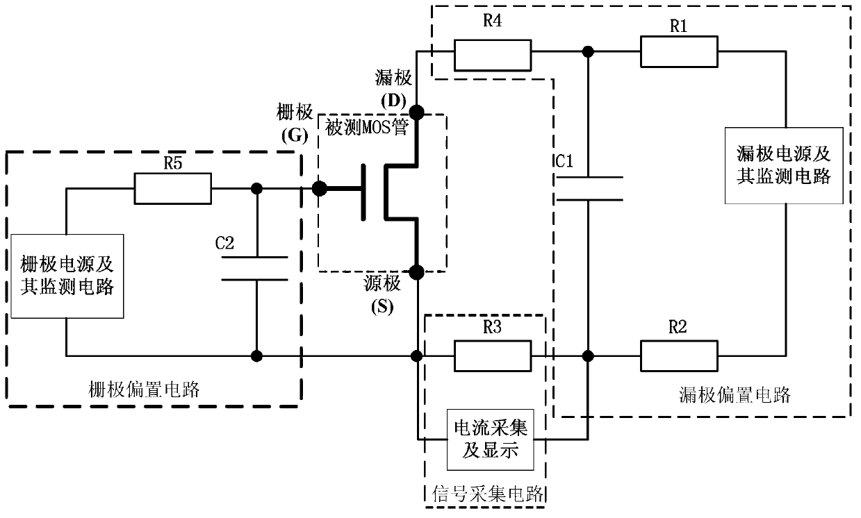
[0026] The invention provides a non-destructive power MOS tube single-event burnout (SEB, single-event burnout) detection circuit and detection method, the circuit is as follows figure 1 As shown, the circuit includes: a gate bias circuit, a drain bias circuit and a signal acquisition circuit.

[0027] The gate bias circuit includes a gate power supply, a gate power supply monitoring circuit, a resistor R5 and a capacitor C2, and the drain bias circuit includes a drain power supply, a drain power supply monitoring circuit, resistors R1, R2, R4 and a capacitor C1, and the signal acquisition The circuit includes a current acquisition display circuit and a resistor R3;

[0028] The positive pole of the gate power supply is connected to the gate of the MOS tube under test through the resistor R5. At the same time, the gate of the MOS tube under test is also connected to the negative pole of the gate power supply and the source of the MOS tube under test through the capacitor C2, w...


PUM


Abstract

The invention discloses a non-destructive power MOS tube single-event burnout effect detecting circuit and a non-destructive power MOS tube single-event burnout effect detecting method. The circuit comprises a grid electrode biasing circuit, a drain electrode biasing circuit and a signal collecting circuit. The method includes the following steps that certain biasing is exerted on a power MOS tube. Currents of a source electrode of the MOS tube are detected under irradiation of heavy ions, and whether single-event burnout of the MOS tube occurs or not is judged through current variation curves. According to performance parameters of a MOS tube device, the source electrode and the drain electrode of the device performs current-limiting on a resistor and discharging and charging on a capacitor so as to keep currents of the source electrode within a detectable range when the single-event burnout happens. Meanwhile, the device is protected against burnout, so that the MOS tube will not be damaged and fail. The method is simple and repeated occurrence of the single-event burnout effect of a MOS tube can be detected. Meanwhile, the feature of being non-destructive is achieved.

Description

technical field [0001] The invention relates to a non-destructive power MOS tube single event burning effect detection circuit and method. Background technique [0002] The power MOS tube is a semiconductor device that uses the electric field effect to control the current. It has a fast switching speed, basically does not need to input the gate current on the control terminal, and has good linear on-resistance, large Current capability and other characteristics; in addition, it is less affected by the external environment, easy to integrate, and widely used in satellite electronic systems. Therefore, the radiation effect of its space environment has also aroused widespread concern. [0003] The single event burnout effect is a catastrophic failure mode of the power MOS tube in the space environment. At present, the ground simulation test method generally adopts the US military standard MIL-STD-750E method 1080. At the same time, the corresponding aerospace standard YHYB B02...

Claims


Application Information

Patent Timeline
Patent Type & Authority Applications(China)
IPC IPC(8): G01R31/26
Inventor 王文炎李鹏伟罗磊于庆奎张磊唐民
Owner CHINA ACADEMY OF SPACE TECHNOLOGY
Learn More