Supercharge Your Innovation With Domain-Expert AI Agents!

Transparent substrate, transparent conductive element and optical device containing the same

A transparent conductive, transparent substrate technology, applied in the field of optics, can solve the problems of affecting the transmission of light and the decrease of touch screen transmittance

Active Publication Date: 2016-06-29
ANHUI JINGZHUO OPTICAL DISPLAY TECH CO LTD
View PDF6 Cites 0 Cited by
  • Summary
  • Abstract
  • Description
  • Claims
  • Application Information

AI Technical Summary

Problems solved by technology

Due to the large difference between the refractive index of the transparent conductive layer and the glass, the light will be reflected and refracted at the interface between the two. Therefore, the transmittance of the touch screen will further decrease, which will affect the transmission of light.

Method used

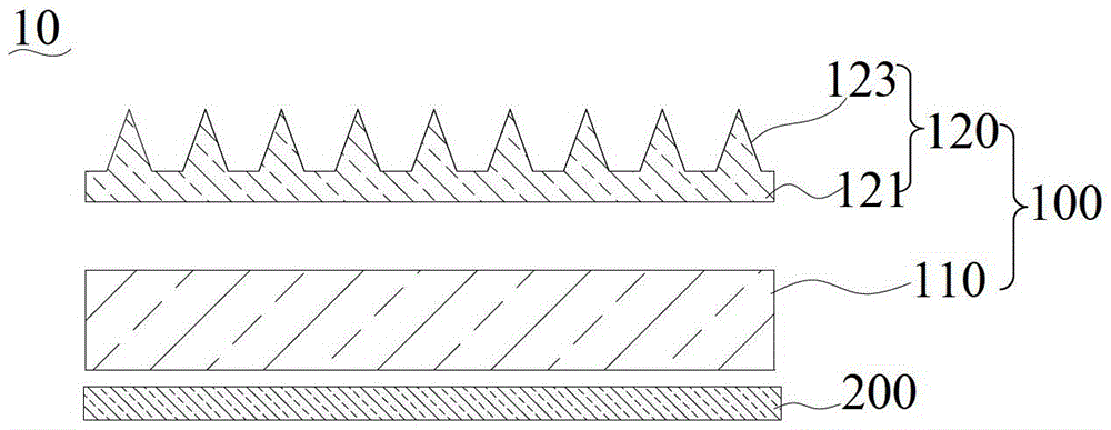
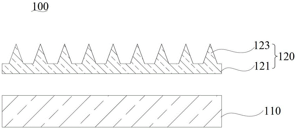
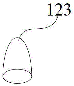

Image

  • Transparent substrate, transparent conductive element and optical device containing the same
  • Transparent substrate, transparent conductive element and optical device containing the same
  • Transparent substrate, transparent conductive element and optical device containing the same

Examples


Embodiment Construction

[0035] In order to facilitate the understanding of the present invention, the present invention will be described more fully below with reference to the associated drawings. Preferred embodiments of the invention are shown in the accompanying drawings. However, the present invention can be embodied in many different forms and is not limited to the embodiments described herein. On the contrary, the purpose of providing these embodiments is to make the disclosure of the present invention more thorough and comprehensive.

[0036] It should be noted that when an element is referred to as being “fixed” to another element, it can be directly on the other element or there can also be an intervening element. When an element is referred to as being "connected to" another element, it can be directly connected to the other element or intervening elements may also be present. The terms "vertical," "horizontal," "left," "right," and similar expressions are used herein for purposes of ill...


PUM

PropertyMeasurementUnit
thicknessaaaaaaaaaa
diameteraaaaaaaaaa
heightaaaaaaaaaa

Abstract

A transparent base material comprises a body and a micro-nano structure formed on one surface of the body. The body is a transparent substrate. The micro-nano structure comprises a plurality of nanoscale protrusions, the protrusions are distributed on the surface of the body in an interval mode, the structural size of each protrusion is smaller than visible light wavelength, so that the protrusion structure cannot be recognized by light waves, therefore, the refractive index of the surfaces of the protrusions changes in a continuous gradient mode, and the reflex phenomenon caused by sharp change of the refractive index can be reduced. The micro-nano structure has good optical reflex reduction effects. When one side, with the micro-nano structure, of the transparent base material is contacted with another optical element in a stacking mode, due to the fact that a micro-nano structure array is of a concave-convex structure and the structure is compact, reflection rays among air clearances will not interfere mutually when contact occurs, and therefore a Newton ring phenomenon can be effectively reduced. The invention further provided a transparent conducting element and an optical device containing the transparent base material.

Description

technical field [0001] The invention relates to the field of optical technology, in particular to a transparent substrate, a transparent conductive element and an optical device containing the transparent substrate. Background technique [0002] The touch screen is an input device that significantly improves the man-machine interface, and has the advantages of intuition, simplicity and speed. Touch screens have been widely used in many electronic products, such as mobile phones, PDAs (Personal Digital Assistants), multimedia, and public information inquiry systems. [0003] The touch screen is usually composed of panel glass and conductive glass components bonded by transparent optical glue. The conductive glass assembly is coated with a transparent conductive layer on one side of the glass substrate. When light passes through a transparent material, due to the refraction and reflection of light, the light that finally passes through the transparent material suffers a cert...

Claims


Application Information

Patent Timeline
Patent Type & Authority Patents(China)
IPC IPC(8): G02B1/116H01B5/14G02B1/11
Inventor 刘伟唐根初唐彬董绳财
Owner ANHUI JINGZHUO OPTICAL DISPLAY TECH CO LTD
Features
  • R&D
  • Intellectual Property
  • Life Sciences
  • Materials
  • Tech Scout
  • Unparalleled Data Quality
  • Higher Quality Content
  • 60% Fewer Hallucinations
Learn More