Thin film transistor, manufacturing method thereof, array substrate and display

A technology of thin film transistors and manufacturing methods, which is applied in the direction of transistors, electric solid-state devices, semiconductor devices, etc., can solve the problems of leakage current and generation of leakage current of thin film transistors, and achieve the effect of high stability characteristics

Inactive Publication Date: 2013-10-23
BEIJING BOE OPTOELECTRONCIS TECH CO LTD
View PDF2 Cites 21 Cited by
  • Summary
  • Abstract
  • Description
  • Claims
  • Application Information

AI Technical Summary

Problems solved by technology

exist figure 2 In the shown top-gate thin film transistor, the gate 600 can block the influence of external light on the semiconductor active layer 400, the drain 200 and the source 300 are disconnected, and the light from the backlight can pass through the transparent substrate 100 The semiconductor active layer 400 is irradiated, and the semiconductor active layer 400 is in contact with the drain electrode 200, a

Method used


Image

  • Thin film transistor, manufacturing method thereof, array substrate and display
  • Thin film transistor, manufacturing method thereof, array substrate and display
  • Thin film transistor, manufacturing method thereof, array substrate and display

Examples


Example Embodiment

[0043] In the specific embodiment of preparing the reflective source electrode, the reflective drain electrode and the metal oxide IGZO semiconductor active layer, the following two implementation schemes are included:

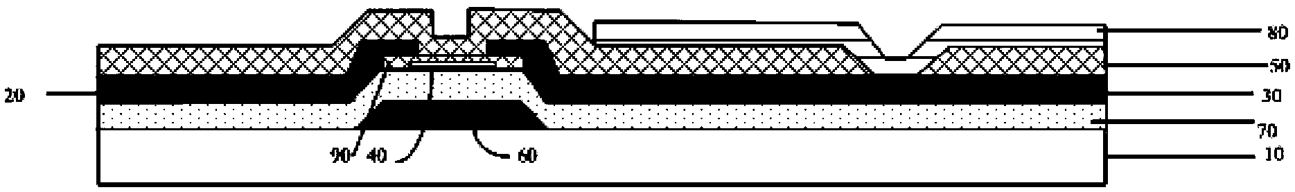
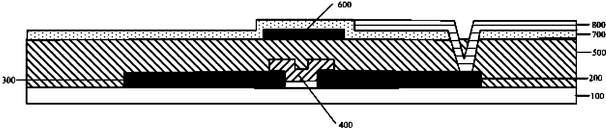
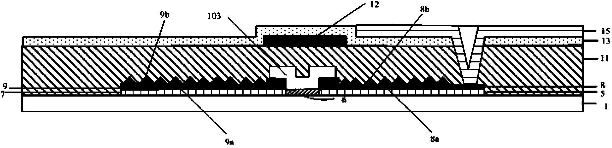
[0044] Option one, in Figure 7 On the basis of, dry etching is used to etch all the metal oxide IGZO semiconductor active layer without photoresist coverage. As the dry etching progresses, the thickness of the photoresist is also reduced accordingly. The thickness of the photoresist 41 covering the region of the metal oxide IGZO semiconductor active layer 102 is relatively thin, and the thickness of the photoresist 42 covering the region of the metal oxide IGZO semiconductor active layer 103 is relatively thick. When the photoresist covering the 102 area is completely etched away to expose the metal oxide IGZO semiconductor active layer, when the dry etching continues at this time, the metal oxide IGZO in the metal oxide IGZO semiconductor active layer 102 area ...


PUM


Abstract

The invention discloses a thin film transistor, a manufacturing method thereof, an array substrate and a display, and aims at solving the problem that the thin film transistor generates leakage current due to a reason that the semiconductor active layer is influenced by illumination. The thin film transistor comprises a source, a drain, a semiconductor active layer, a grid insulating layer and a grid. The thin film transistor further comprises a visor is arranged between the source and the drain. The visor obstructs the source from the drain. Besides, the visor is arranged on the side of the incident light of the semiconductor active layer and is used for obstructing the incident light from irradiating the semiconductor active layer.

Description

technical field [0001] The invention relates to the technical field of displays, in particular to a thin film transistor, a manufacturing method thereof, an array substrate and a display. Background technique [0002] figure 1 It is a schematic structural diagram of a bottom-gate thin film transistor (Thin Film Transistor, TFT) in the prior art, and the thin film transistor includes: a gate 60 formed on a base substrate 10, a gate insulating layer 70, a source 20, and a drain 30 . The semiconductor active layer 40 and the protective layer 90 . The array substrate containing thin film transistors also includes a passivation layer 50 and a pixel electrode 80 . The gate 60 of the bottom-gate thin film transistor can block the light from the backlight, and prevent the semiconductor active layer 40 from being illuminated by the backlight to cause leakage current of the thin film transistor. In order to avoid the impact of water and oxygen in the external environment on the sem...

Claims


Application Information

Patent Timeline
IPC IPC(8): H01L21/336H01L29/786H01L29/06
CPCH01L29/78633H01L27/1262H01L29/41733H01L29/45H01L29/458H01L29/66969H01L29/7869
Inventor 阎长江蒋晓纬姜晓辉谢振宇陈旭
Owner BEIJING BOE OPTOELECTRONCIS TECH CO LTD
Why Eureka
Try Eureka