
Three-dimensional stack package structure of semiconductor devices with double-sided water cooling of fixtures

A technology for fixing devices and packaging structures, which is applied in semiconductor devices, semiconductor/solid-state device parts, electric solid-state devices, etc. It can solve the problems of aluminum alloys not meeting the requirements, heat dissipation requirements, and large volume of planar packaging. The effect of large size, small size and large heat dissipation coefficient

Inactive Publication Date: 2016-12-14
NANJING HIGHSEMI ELECTRIC POWER SCI & TECH CO LTD
View PDF4 Cites 0 Cited by
  • Summary
  • Abstract
  • Description
  • Claims
  • Application Information

AI Technical Summary

Problems solved by technology

[0003] At present, the volume and weight of the semiconductor element planar package used in the traditional structure and the aluminum alloy heat sink do not meet the requirements. On the one hand, the planar package occupies a large volume, and a large number of lead wires are required for packaging, which brings a large number of leads. resistance and self-generated inductance, thereby increasing the heat generation and improving the failure rate; on the other hand, the traditional heat sink structure cannot meet the heat dissipation requirements in large power devices, and requires a larger heat sink structure

Method used


Image

  • Three-dimensional stack package structure of semiconductor devices with double-sided water cooling of fixtures
  • Three-dimensional stack package structure of semiconductor devices with double-sided water cooling of fixtures
  • Three-dimensional stack package structure of semiconductor devices with double-sided water cooling of fixtures

Examples


Embodiment 1

[0028] Further illustrate this embodiment below in conjunction with accompanying drawing:

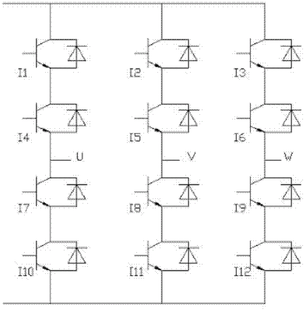
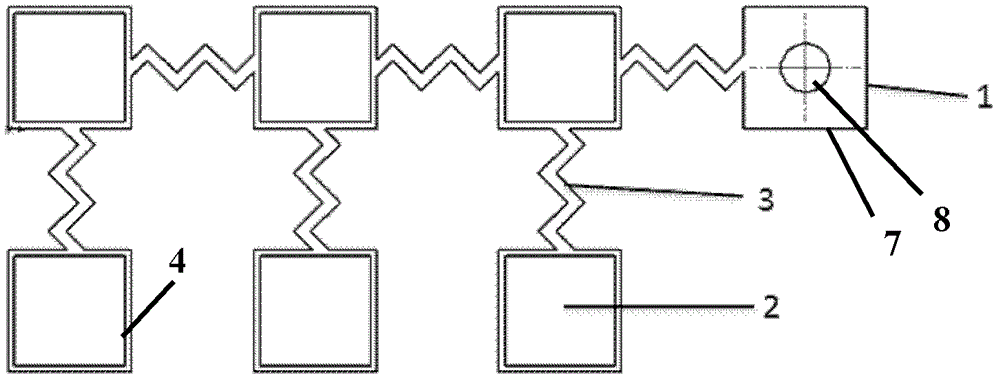
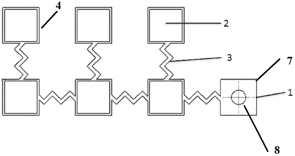
[0029] Referring to Fig. 2 to Fig. 7, this embodiment is a three-dimensional intelligent packaging structure of a semiconductor device with double-sided water cooling with a fixing device. Circuit structure diagram see figure 1 , I1-I12 are 12 semiconductor chips, which are divided into four layers of stacking, and each layer has three chips. The structure consists of three laminated boards and two laminated boards, which are cross-stacked. See Figure 2 and Figure 3. Each laminated board contains 6 unit boards 2 . The laminated board 1 is formed by stamping or forging, and the upper and lower surfaces are processed with grooves 4. The grooves 4 are "mouth"-shaped structures distributed around the unit board 2, and the topmost laminated board 1 only has grooves 4 on the lower surface. , the laminated board 1 at the bottom has only grooves 4 on the upper surface, and the grooves 4 are...

Embodiment 2

[0031] Embodiment 2 is the same as Embodiment 1, except that the water-cooling channel is serpentine. A substrate with a built-in serpentine water-cooling channel is placed on the upper and lower surfaces of the stacked structure, see Figure 8. Continuous pressure is applied to the monolithic structure by means of bolted connections, see Figure 9.

Embodiment 3

[0033] Embodiment 3 is the same as Embodiment 1, except that the water-cooling channels are tree-shaped. A substrate with built-in tree-shaped water-cooling channels is placed on the upper and lower surfaces of the stacked structure, see Figure 10. Continuous pressure is applied to the monolithic structure by means of bolted connections, see Figure 11.


PUM


Abstract

Disclosed is a three-dimensional stacked encapsulation structure of a double-face water-cooling semiconductor component with fixing devices. The structure includes lamination plates, positioning devices in the lamination plates, connecting pieces in the lamination plates, wire leading terminals, substrates, temperature and pressure measurement devices and water cooling channels. The structure is characterized in that: the lamination plates are comprised by unit plates and the transformable connecting pieces; the three-dimensional stacked encapsulation structure is formed by laminating a plurality of lamination plates; a positioning device is arranged and a plurality of semiconductor components are encapsulated in each lamination plate; each lamination plate is provided with the temperature and pressure measurement devices; the upper ends and the lower ends of the lamination plates are provided with substrates; the water cooling channels are arranged in the substrates; and the encapsulation structure is provided with the semiconductor components wire leading terminals. The structure is small in size, large in power which can be integrated, and high in heat dissipation coefficient; the structure has the characteristics of shock and vibration resistance and expansion with heat and contraction with coldness; and each lamination plate is provided with the temperature and pressure measurement devices.

Description

technical field [0001] The invention relates to a semiconductor device, in particular to a three-dimensional intelligent packaging structure of a semiconductor device with double-sided water cooling with a fixing device. Background technique [0002] Semiconductor devices, especially high-power semiconductor devices, are widely used in weak and strong current fields. With the development of power devices, how to reduce the weight and volume of power devices and solve the heat dissipation problems caused by the accompanying high power density has attracted extensive attention in the industry. The three-dimensional packaging form of semiconductor devices and the efficient cooling structure design become the key factors for the reduction of device weight and volume. [0003] At present, the volume and weight of the semiconductor component planar package used in the traditional structure and the aluminum alloy heat sink do not meet the requirements. On the one hand, the planar ...

Claims


Application Information

Patent Timeline
Patent Type & Authority Patents(China)
IPC IPC(8): H01L23/473
CPCH01L2924/0002
Inventor 刘胜徐玲吴林
Owner NANJING HIGHSEMI ELECTRIC POWER SCI & TECH CO LTD
Learn More