
SMD type passive electronic component mounting structure and method

A technology for electronic components and mounting structures, which is applied in the field of patch-type passive electronic component mounting structures and methods, can solve problems such as void layering, short circuit of component terminals, and inability to adhere to chips, so as to eliminate gaps, improve precision and reliability sexual effect

Active Publication Date: 2017-03-29
HANGZHOU SILAN INTEGRATED CIRCUIT
View PDF8 Cites 0 Cited by
  • Summary
  • Abstract
  • Description
  • Claims
  • Application Information

AI Technical Summary

Problems solved by technology

[0006] c: Traditional SMT and reflow soldering equipment cannot adapt to the installation and welding of patch-type passive electronic components with a length of less than 0.6mm, and it is easy to cause problems such as short circuits between component terminals, such as Figure 5 shown; on the other hand, if the SMD passive electronic component is offset from the pad, there will be an open circuit problem, such as Image 6 shown;
[0007] d: There will be tiny gaps 90 below the SMD passive electronic components, it is difficult to fill the potting compound, and it is easy to produce abnormalities such as void delamination
[0008] f: When a variety of patch-type passive electronic components and integrated circuit chips are packaged together, the patch-type passive electronic components cannot be stacked on other electronic components or chips, usually only such as Figure 7 As shown in the installation structure, when multiple electronic components are combined at the same time, the circuit terminals are affected by the size of various electronic components, making it difficult to design and layout;
[0009] g: In the chip-level package, the SMD thermistor is affected by the size and welding method, and can only be electrically connected to the chip through the circuit terminal, and cannot be attached to the chip, resulting in the resistor being unable to sense the actual temperature of the chip surface and measuring data large deviation
[0010] Due to the above problems, for the existing chip-type passive electronic components, especially for the chip-type thermistor used in MEMS products, the installation structure and installation method still need to be improved

Method used


Image

  • SMD type passive electronic component mounting structure and method
  • SMD type passive electronic component mounting structure and method
  • SMD type passive electronic component mounting structure and method

Examples


no. 1 example

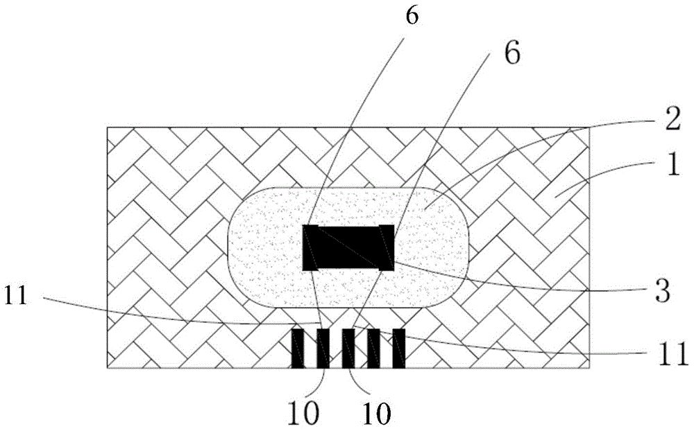
[0036] Below, refer to Figure 1A , Figure 1B and figure 2 The installation structure according to the first embodiment of the present invention is explained, wherein Figure 1A and Figure 1B is a schematic diagram of the mounting structure at different stages of fabrication, figure 2 It is a top view of the installation structure. The first embodiment of the present invention is a mounting structure in which a chip thermistor 3 is mounted on a substrate 1 as a passive electronic component.

[0037] Such as Figure 1A As shown, a substrate 1 is provided as a carrier part, and a high thermal conductivity insulating glue 2 is first dotted on the substrate 1, and then, as shown in FIG. Figure 1B As shown in , paste the chip thermistor 3 on the high thermal conductivity insulating glue 2, and fix the insulating glue 2. The amount of glue dispensing can be set according to the size of the chip thermistor 3. It is best that the high thermal conductivity insulating glue 2...

no. 2 example

[0044] image 3 A schematic diagram showing a mounting structure according to a second embodiment of the present invention. The difference from the first embodiment is that an electronic component 4 as a carrier part is added in the mounting structure of the second embodiment, and the electronic component 4 can be an active electronic component, such as an integrated circuit chip, or another A surface mount passive electronic component such as a resistor, inductor or capacitor. One surface of the electronic component 4 as the carrier part is pasted on the substrate 1 by insulating glue 7, and the chip type thermistor 3 is pasted on the other surface of the electronic component 4 as the carrier part by the high thermal conductivity insulating glue 2, usually On the upper surface of the second electronic component 4 .

[0045] In addition, the mounting structure of the second embodiment also includes bonding wires 11 for electrical connection. Specifically, the mounting struc...

no. 3 example

[0051] Figure 4 A schematic diagram of a mounting structure according to a third embodiment of the present invention is shown. The mounting structure of the third embodiment uses the integrated circuit chip 5 as the carrier part of the chip thermistor 3 . In particular, here the integrated circuit chip 5 is configured to have a groove 20 , and the chip thermistor 3 is fixed in the groove 20 by the high thermal conductivity insulating glue 2 . The groove 20 can be formed in the integrated circuit chip 5 by an etching method. Preferably, the depth of the groove 20 can be set to be larger than the height of the thermistor 3, so that the thermistor 3 is completely accommodated in the groove 20 and It does not protrude from the upper surface of the integrated circuit chip 5 . Two terminals 6 of the thermistor 3 are connected to pads 12 as terminals on the integrated circuit chip 5 through bonding wires 11 .

[0052] The installation method of the installation structure of the t...


PUM


Abstract

The invention relates to an installation structure and method of a surface mount type passive electronic component. The installation structure of the surface mount type passive electronic component with terminals comprises a carrier part, insulating glue for fixing the surface mount type passive electronic component to the carrier part, and a bonding wire with one end being bonded to one of the terminals of the surface mount type passive electronic component. The installation method comprises the following steps: providing the carrier part; fixing the surface mount type passive electronic component to the carrier part by the insulating glue; and connecting one end of the bonding wire to one of the terminals of the surface mount type passive electronic component through a bonding technology so as to realize electrical connection. By virtue of the installation structure and the installation method, a capsulation structure with high density, high precision and high moldability can be achieved.

Description

technical field [0001] The invention relates to a mounting structure and a mounting method of a chip-type passive electronic component, in particular to a mounting structure and a mounting method of a chip-type passive electronic component used in MEMS (micro-electromechanical system) products. Background technique [0002] MEMS refers to a micro device or system that can be produced in batches, integrating micro mechanisms, micro sensors, micro actuators, signal processing and control circuits, up to interfaces, communications and power supplies. A large number of SMD passive electronic components need to be integrated in MEMS. The so-called passive electronic components refer to those electronic components that can display their characteristics without the need for an external power supply. Passive components are mainly resistive, inductive and capacitive electronic components, and their common feature is that they can work when there is a signal without adding power to t...

Claims


Application Information

Patent Timeline
Patent Type & Authority Patents(China)
IPC IPC(8): H01C1/01H01C7/00
Inventor 李学敏丁立国周润宝
Owner HANGZHOU SILAN INTEGRATED CIRCUIT
Learn More