Waterproof wafer-level package method aiming at glass-silicon-glass sandwich structure
A wafer-level packaging and sandwich technology, which is applied to reduce the impact of water flow, and achieves the effect of preventing the impact of water flow, and the size and depth of the structure are precisely controllable.
- Summary
- Abstract
- Description
- Claims
- Application Information
AI Technical Summary
Problems solved by technology
Method used
Image
Examples
Embodiment Construction
[0037] In order to prevent the scribing water from flowing into the layout design, there are no graphics and structures within 5mm of the edges of the three wafers during the layout design, so as to ensure that the edges of the wafers can be bonded firmly during the two anodic bonding, and the water will not flow during scribing. It enters the interior of the device from the side of the three-layer wafer stack.
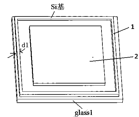
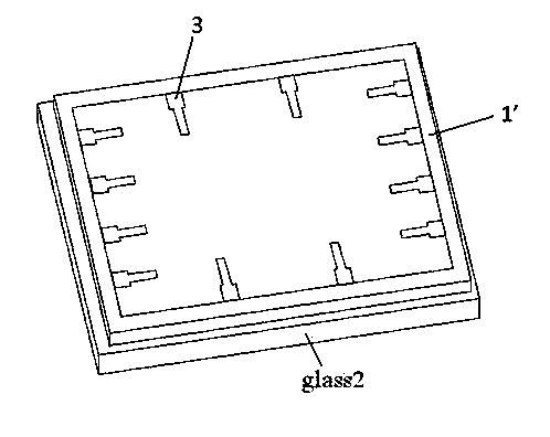
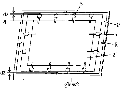
[0038] Control attached figure 1 After the front structure of the silicon-based structure wafer Si is completed, the first anodic bonding is performed with the sealing glass wafer glass1, and the sealing glass wafer glass1 can be used as a supporting substrate for the silicon-based structure 2 of the device. Use the overlay process to register the back and front patterns of the silicon wafer, and then perform dry etching and structure release of the chip unit silicon base structure 2 and the wall structure 1, so that the unnecessary silicon base is etched away, and the ...
PUM
| Property | Measurement | Unit |
|---|---|---|
| thickness | aaaaa | aaaaa |
Abstract
Description
Claims
Application Information
 - R&D
- Intellectual Property
- Life Sciences
- Materials
- Tech Scout
- Unparalleled Data Quality
- Higher Quality Content
- 60% Fewer Hallucinations
Browse by: Latest US Patents, China's latest patents, Technical Efficacy Thesaurus, Application Domain, Technology Topic, Popular Technical Reports.
© 2025 PatSnap. All rights reserved.Legal|Privacy policy|Modern Slavery Act Transparency Statement|Sitemap|About US| Contact US: help@patsnap.com


