
A transistor base and a transistor hermetic packaging structure

A technology of transistors and stems, which is applied in the field of transistor stems and transistor hermetic packaging structures, can solve the problems of high speed, reduced size, and low cost of TO stems, and achieve stable packaging structure, reduced size, and convenient chip packaging Effect

Active Publication Date: 2022-03-11
WUHAN UF OPTOELECTRIC TECH CO LTD
View PDF11 Cites 0 Cited by
  • Summary
  • Abstract
  • Description
  • Claims
  • Application Information

AI Technical Summary

Problems solved by technology

[0004] In order to solve the problem that the existing TO stem and transistor cannot be further reduced in size due to the design of the glass-metal package shell, the purpose of the present invention is to provide a new type of transistor stem and transistor hermetic packaging structure, which can solve the problem of TO stem height With high speed, high heat dissipation and low cost, the size of TO tube base and transistor can continue to be reduced to achieve the purpose of miniaturization

Method used


Image

  • A transistor base and a transistor hermetic packaging structure
  • A transistor base and a transistor hermetic packaging structure
  • A transistor base and a transistor hermetic packaging structure

Examples


Embodiment 1

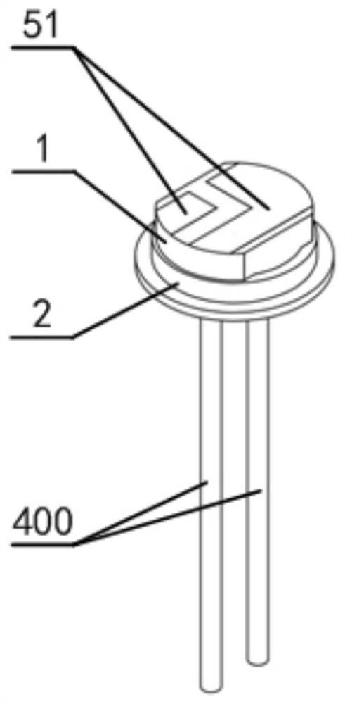
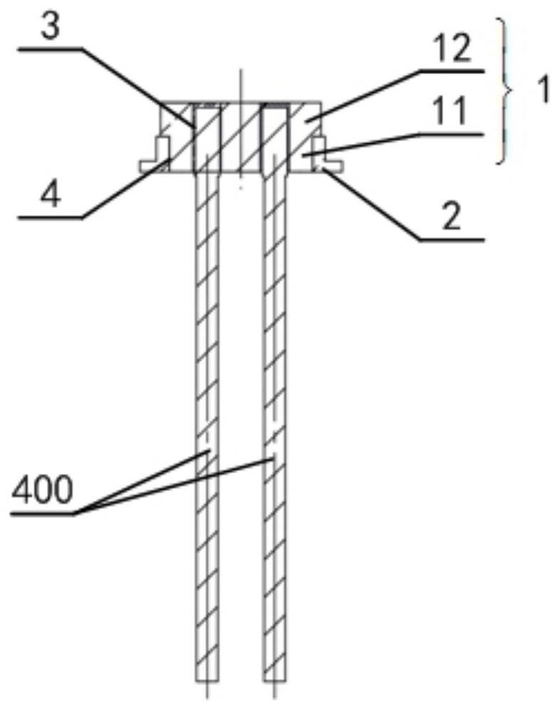
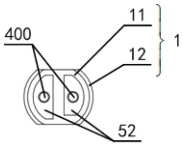
[0052] Such as Figure 1~3 As shown, the first transistor base provided in this embodiment includes an insulating base 1 and a circumferentially closed metal base 2, wherein the top surface of the insulating base 1 is used to place a transistor chip 300; the insulating base 1 is provided with at least one conductive channel 3, and the outer peripheral surface of the insulating base 1 is sealed and connected to the inner ring surface of the circumferentially closed metal base 2 through a filler 4, wherein the top end of the conductive channel 3 is used for a The chip pins of the transistor chip 300 are electrically connected one by one, and the bottom end of the conductive channel 3 is used for electrically connecting the external wiring parts of the transistor one by one.

[0053] Such as Figure 1~3 As shown, in the specific structure of the transistor base, the insulating base 1 is used to realize the circumferential sealing between the metal base 2 and the conductive chann...

Embodiment 2

[0062] Such as Figure 4~6 As shown, on the basis of the technical solution of the first embodiment, this embodiment provides the second transistor base, which differs from the first transistor base described in the first embodiment in that there is no transistor pin 400 It is designed that the second conductive pad 52 is directly used as the external connection member of the transistor corresponding to the conductive channel 3 . For example, when a conventional diode chip is packaged in the tube, one of the second conductive pads 52 can be used as an anode pad, and the other second conductive pad 52 can be used as a cathode pad, which can also be conveniently used in actual circuit boards.

[0063] The technical effect of this embodiment can be directly derived by referring to the technical effect of the first embodiment, and will not be repeated here.

Embodiment 3

[0065] Such as Figure 7 As shown, this embodiment provides a third type of transistor base on the basis of the technical solution of Embodiment 1, which is different from the first type of transistor base in Embodiment 1 in that: the conductive channel 3 The top surface protrudes from the top surface of the insulating base 1, the first conductive pad 51 is arranged on the top surface of the conductive channel 3; the transistor chip 300 is arranged on the top surface of the insulating base 1 , and connect the chip pins on the transistor chip 300 and the first conductive pad 51 through gold wires; the insulating base 1 and the filler 4 are sealed with the ring-to-enclosed metal base 2 using the same material .

[0066] Optimally, the transistor chip 300 is disposed on the first conductive pad 51 located on the top surface of the conductive channel 3 .

[0067] The technical effect of this embodiment can be directly derived by referring to the technical effect of the first emb...


PUM


Abstract

The invention relates to the technical field of transistor packaging, and discloses a transistor base and a transistor hermetic packaging structure. The transistor base includes an insulating base and a circumferentially closed metal base, wherein the top surface of the insulating base is used to place a transistor chip; the inside of the insulating base is provided with at least one conductive channel, and the outer peripheral surface of the insulating base is It is connected with the inner ring surface of the circumferentially closed metal base by packing seal. Through the transistor base, while solving the problem of high speed, high heat dissipation and low cost of the TO base, the size of the TO base and the transistor can be continuously reduced, thereby achieving the purpose of miniaturization. In addition, through the transistor hermetic packaging structure, three-dimensional packaging of multi-transistor chips can be realized, which is further beneficial to reducing the size of the transistor packaging structure.

Description

technical field [0001] The invention relates to the technical field of transistor packaging, in particular to a transistor base and a transistor hermetic packaging structure. Background technique [0002] TO socket (TO is the English abbreviation of TRANSISTOR OUTLINE of the transistor shell) is widely used in the field of optoelectronic communication. In order to meet the growing demand for high transmission speed, low cost, high heat dissipation and small size, etc., TO glass-metal packaging has become the mainstream design in the market. The specific preparation methods are as follows: (1) KOVAR (Kovar) Alloy, also known as iron-nickel-cobalt alloy) base, radio frequency lead and low dielectric constant glass matching the thermal expansion coefficient; (2) stainless steel base, radio frequency lead and high dielectric constant glass matching the thermal expansion coefficient encapsulation. However, for TO shells with KOVAR alloy bases, due to the low thermal conductivit...

Claims


Application Information

Patent Timeline
Patent Type & Authority Patents(China)
IPC IPC(8): H01L23/055H01L23/10H01L23/13H01L23/31H01L33/48H01L33/62H01L33/64H01L33/54
CPCH01L23/055H01L23/10H01L23/13H01L23/3107H01L33/483H01L33/62H01L33/54H01L33/641
Inventor 张迪
Owner WUHAN UF OPTOELECTRIC TECH CO LTD
Learn More