Avalanche photodiode and method for manufacturing the same

An avalanche optoelectronics and manufacturing method technology, applied in photovoltaic power generation, circuits, electrical components, etc., can solve the problems of carrier movement obstruction, valence band/conduction band energy level discontinuity, poor high-speed response, etc.

Inactive Publication Date: 2013-11-13
MITSUBISHI ELECTRIC CORP
View PDF9 Cites 5 Cited by
  • Summary
  • Abstract
  • Description
  • Claims
  • Application Information

AI Technical Summary

Problems solved by technology

[0017] In addition, in the conventional avalanche photodiode, the energy level discontinuity of the valence band / conduction band at the interface between the window layer and the light absorbing layer is large, and the movement of carriers is hindered, so there is a problem that the high-speed response is poor. question

Method used


Image

  • Avalanche photodiode and method for manufacturing the same
  • Avalanche photodiode and method for manufacturing the same
  • Avalanche photodiode and method for manufacturing the same

Examples


Embodiment approach 1

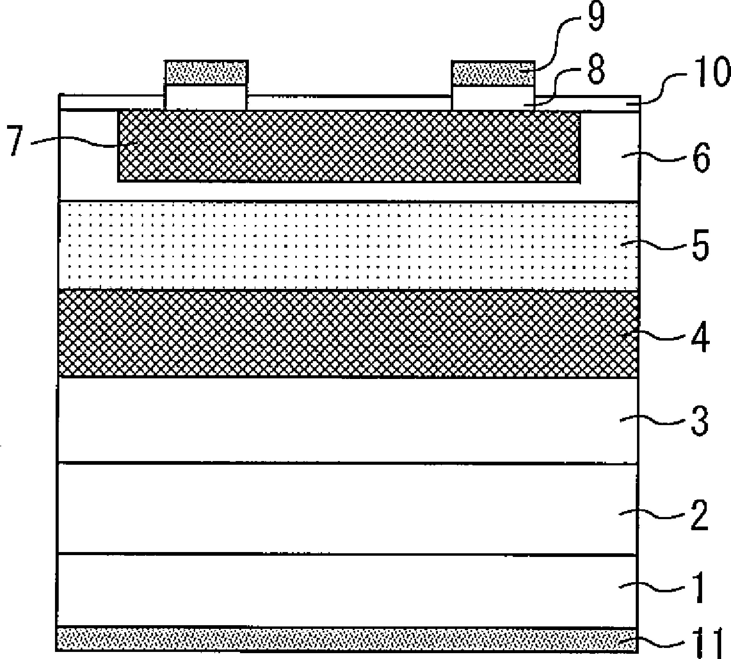
[0033] figure 1 is a cross-sectional view showing the avalanche photodiode according to Embodiment 1 of the present invention. On the n-type InP substrate 1, an n-type AlInAs buffer layer 2, an AlInAs avalanche multiplication layer 3, a p-type AlInAs electric field control layer 4, an undoped light absorbing layer 5 and a window layer 6 are sequentially laminated. Carbon is used as a dopant for the p-type AlInAs electric field control layer 4 .

[0034] The carrier concentration of the n-type AlInAs buffer layer 2 is 5×10 18 cm -3 Hereinafter, the layer thickness is 0.1 to 1 μm. The carrier concentration of AlInAs avalanche multiplication layer 3 is 0.1×10 15 ~8×10 15 cm -3 , the layer thickness is 0.05-0.5 μm. The carrier concentration of the p-type AlInAs electric field control layer 4 is 2×10 17 ~2×10 18 cm -3 , the layer thickness is 0.01-0.2 μm. The layer thickness of the undoped light absorbing layer 5 is 0.5-2.5 μm. The window layer 6 is not doped or doped a...

Embodiment approach 2

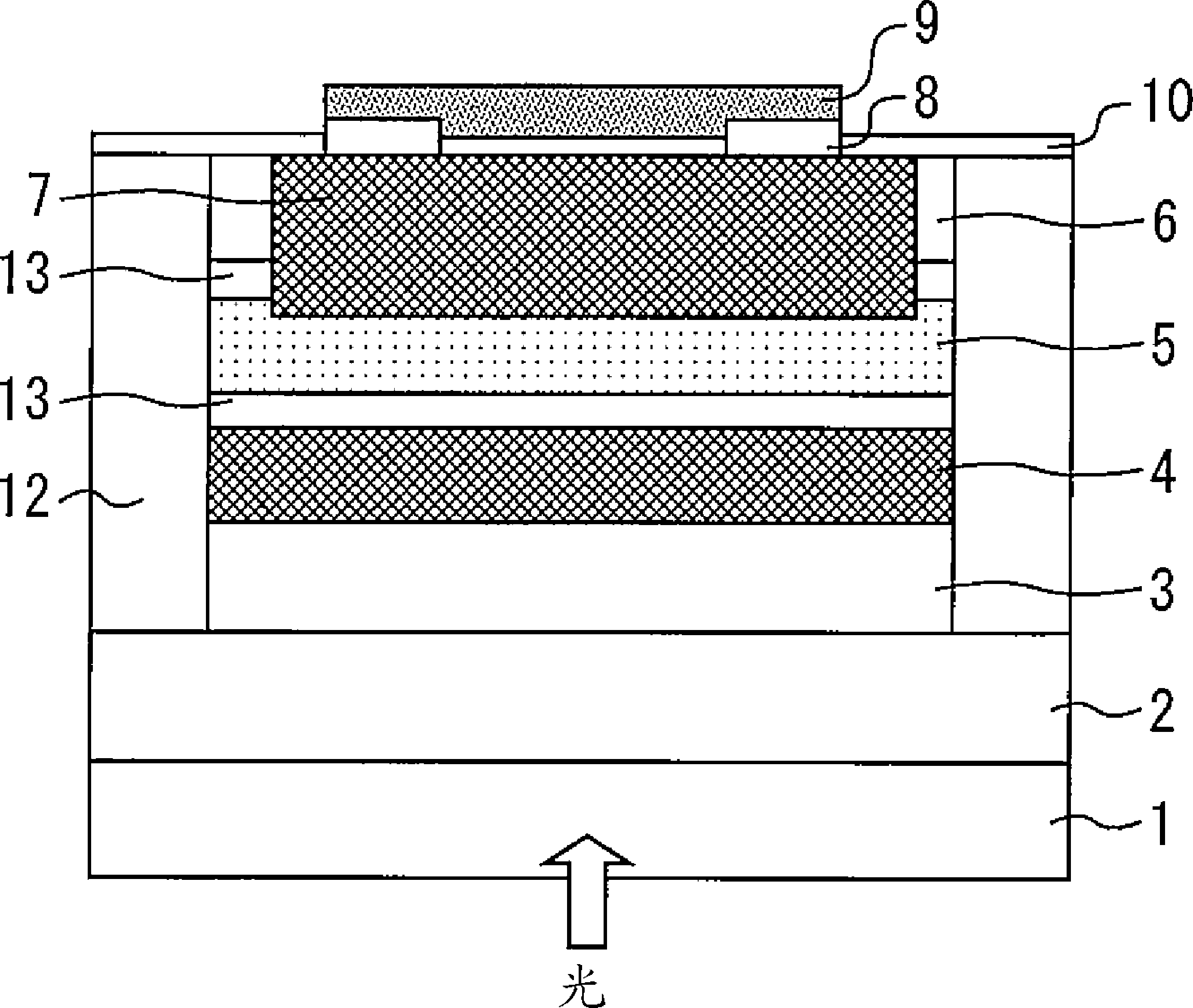
[0052] Figure 5 is a cross-sectional view showing an avalanche photodiode according to Embodiment 2 of the present invention. The semi-insulating buried semiconductor layer 12 is buried in the sides of the AlInAs avalanche multiplication layer 3 , the p-type AlInAs electric field control layer 4 , the undoped light absorbing layer 5 and the window layer 6 . However, it is only necessary that the embedded semiconductor layer 12 is embedded in at least the undoped light absorbing layer 5 . The buried semiconductor layer 12 has a wider band gap than the undoped light absorbing layer 5 .

[0053] The embedded semiconductor layer 12 can prevent the undoped light absorbing layer 5 with a narrow band gap from being exposed, and improve device reliability. Furthermore, since the undoped window layer 6 exists between the p-type region 7 and the buried semiconductor layer 12, leakage current does not increase.

Embodiment approach 3

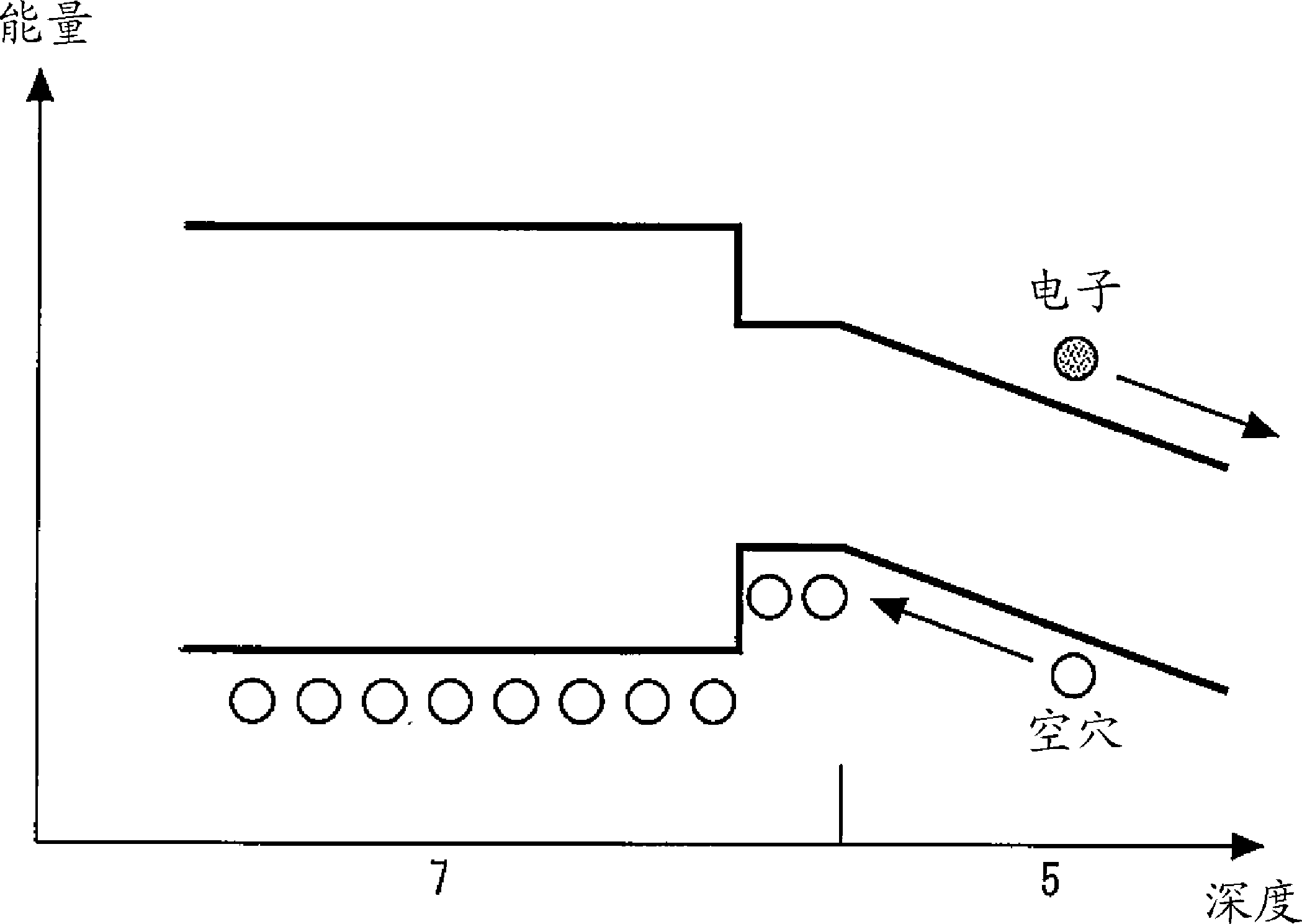
[0055] Figure 6 is a cross-sectional view showing an avalanche photodiode according to Embodiment 3 of the present invention. A graded layer 13 is provided between the undoped light absorbing layer 5 and the adjacent layer. Other structures are the same as those in Embodiment 2. Thereby, the discontinuity between the valence band and the conduction band between the undoped light absorbing layer 5 and the adjacent layer becomes small, and the movement of carriers becomes easy, so that high-speed response can be improved. In addition, although it is preferable that the graded layer 13 is located on both sides of the undoped light-absorbing layer 5, it is effective even if it is located on only one side.


PUM


Abstract

The invention relates to an avalanche photodiode and a method for manufacturing the same. The avalanche photodiode can improve high-speed response and reduce the features changing along time. The avalanche photodiode includes a N-type Inp substrate; an allnAs avalanche multiplying layer (3), a p-type electric field controlling layer (4), a non-doping light-absorbing layer (5), and a window layer (6) sequentially laminated on the substrate. A p-type region is present in parts of the window layer (6) and the non-doping light-absorbing layer (5). Carbon is the dopant of the electric field controlling layer (4). Zn is the dopant of the p-type region. A bottom face of the p-type region is closer to the substrate than is an interface between the non-doping light-absorbing layer (5) and the window layer (6).

Description

technical field [0001] The present invention relates to an avalanche photodiode used in optical fiber communication and the like and a method of manufacturing the same. Background technique [0002] An avalanche diode (avalanche diode) has a light absorbing layer and an avalanche multiplication layer. When light enters the light-absorbing layer, electron-hole pairs are generated. When they become carriers and reach the avalanche multiplication layer, the multiplication of carriers occurs avalanche-like. As a result, incident light can be amplified and taken out as a signal. Therefore, avalanche diodes are often used in long-distance optical communications for receiving weak optical signals. [0003] In order to cause avalanche multiplication, a high electric field needs to be applied to the avalanche multiplication layer. However, when a high electric field is applied to the light-absorbing layer, tunnel breakdown occurs in the light-absorbing layer. Therefore, an electr...

Claims


Application Information

Patent Timeline
Patent Type & Authority Applications(China)
IPC IPC(8): H01L31/107H01L31/0304H01L31/0352H01L31/18
CPCH01L31/1844H01L31/107H01L31/18Y02E10/544H01L31/1075
Inventor 竹村亮太石村荣太郎
Owner MITSUBISHI ELECTRIC CORP
Why Eureka
Try Eureka