image display device

A technology for image display devices and pixel circuits, which can be applied to static indicators, instruments, etc., and can solve the problems of shortened writing operation time and difficult high-definition image display devices, etc.

Inactive Publication Date: 2016-06-29
JOLED INC
View PDF8 Cites 0 Cited by
  • Summary
  • Abstract
  • Description
  • Claims
  • Application Information

AI Technical Summary

Problems solved by technology

[0007] However, in the pixel circuits and their driving methods described in Patent Documents 1 and 2, since the correction operation of the threshold voltage is performed using the data line supplying the image signal, the time available for the write operation is shortened, so it is difficult to realize a large number of pixels. Large-screen image display device or high-definition image display device

Method used


Image

  • image display device
  • image display device
  • image display device

Examples


Embodiment approach 1

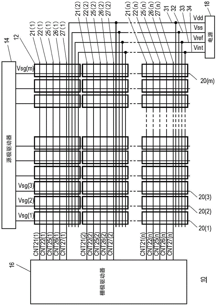
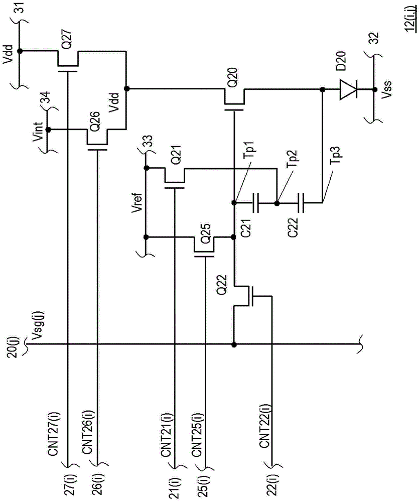
[0028] figure 1 It is a schematic diagram showing the configuration of the image display device 10 in the first embodiment. The image display device 10 in this embodiment has a plurality of pixel circuits 12 (i, j) (where: 1≤i≤n, 1≤j≤m) arranged in a matrix of n rows and m columns, a source driver circuit 14 , gate driver circuit 16 and power supply circuit 18 .

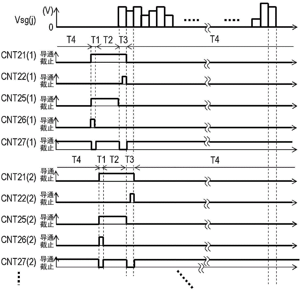
[0029] source driver circuit 14 to figure 1 The data lines 20(j) to which the pixel circuits 12(1,j) to 12(n,j) arranged in the column direction are commonly connected provide the image signal voltage Vsg(j) independently. In addition, the gate driver circuit 16 to figure 1 The control signal lines 21(i), 22(i), 25(i), 26(i), 27( i) Provide control signals CNT21(i), CNT22(i), CNT25(i), CNT26(i), CNT27(i) respectively. In this embodiment, five types of control signals are supplied to one pixel circuit 12(i, j), but the number of control signals is not limited thereto, and it is only necessary to supply as many co...

Embodiment approach 2

[0074] The structure of the image display device 10 in Embodiment 2 and figure 1 Embodiment 1 shown in is substantially the same. Embodiment 2 differs from Embodiment 1 in the configuration of pixel circuits 12 (i, j). The pixel circuit in Embodiment Mode 2 has an independent circuit provided independently for each organic EL element D20 that is a current light emitting element, and a common circuit provided commonly for a plurality of current light emitting elements.

[0075] Figure 9 is a circuit diagram of the pixel circuit of the image display device 10 in Embodiment 2, and shows three independent circuits 42(i, j-1), 42(i, j), 42(i, j+1) and their common Circuit 50. The independent circuit 42 (i, j) in Embodiment 2 includes: an organic EL element D20 as a current light-emitting element, a drive transistor Q20, a first capacitor C21, a second capacitor C22, a transistor Q21 as a first switch, and Transistor Q22 as the second switch, and transistor Q25 as the fifth swi...

Embodiment approach 3

[0090] Figure 10 is a circuit diagram of the pixel circuit of the image display device 10 in Embodiment 3, and shows three independent circuits 42(i, j-1), 42(i, j), 42(i, j+1) and their common Circuit 60. Since the configuration and operation of the independent circuit 42(i, j) are the same as those of the independent circuit 42(i, j) in Embodiment 2, detailed description thereof will be omitted.

[0091] Common circuit 60 in Embodiment Mode 3 and Figure 9 The common circuit 50 shown in is the same, the drain (or source) of the transistor Q56 as the 3rd switch is connected to the node Tp40, the source (or drain) of the transistor Q56 is connected to the voltage line 34, and the transistor Q56 The gate of is connected to the control signal line 26(i). In addition, the source of the transistor Q67 serving as a fourth switch is connected to the node Tp40, the drain of the transistor Q67 is connected to the power supply line 31, and the gate of the transistor Q67 is connecte...


PUM


Abstract

The pixel circuit (12) in the present invention is provided with: a first capacitor (C21) with one terminal connected to the gate of the driving transistor (Q20); The second capacitor (C22) between the second capacitor (C22); the first switch (Q21) that applies the reference voltage Vref to the node Tp2 of the first capacitor (C21) and the second capacitor (C22); provides an image signal to the gate of the drive transistor (Q20) The second switch (Q22) for the voltage Vsg; the third switch (Q26) for supplying the initialization voltage Vint to the drain of the driving transistor (Q20); 4th switch (Q27).

Description

technical field [0001] The present invention relates to an active matrix image display device using a current light-emitting element. Background technique [0002] An organic EL display device in which a plurality of self-luminous organic electroluminescent (hereinafter referred to as "organic EL") elements is arranged is considered as a next-generation image display device because it does not require a backlight and has no limitation on the viewing angle. Advance development. [0003] An organic EL element is a current light-emitting element whose brightness is controlled by the amount of current flowing through it. As a method for driving an organic EL element, there are a passive matrix method and an active matrix method. Although the former has a simple pixel circuit, it is difficult to realize a large-scale and high-definition display. Therefore, an active-matrix organic EL display device in which driving transistors are arranged in each pixel circuit has gradually b...

Claims


Application Information

Patent Timeline
Patent Type & Authority Patents(China)
IPC IPC(8): G09G3/30G09G3/20
CPCG09G3/3233G09G3/3291G09G2300/0819G09G2300/0852G09G2300/0861G09G2310/0262G09G2310/067G09G2320/043G09G3/20G09G3/30
Inventor 柘植仁志
Owner JOLED INC
Why Eureka
Try Eureka