image display device

A technology for image display devices and pixel circuits, which is applied to static indicators, instruments, electric solid devices, etc., and can solve problems such as difficult high-definition image display devices and shortened writing operation time

Active Publication Date: 2016-08-17
JOLED INC
View PDF8 Cites 0 Cited by
  • Summary
  • Abstract
  • Description
  • Claims
  • Application Information

AI Technical Summary

Problems solved by technology

[0007] However, in the pixel circuit and its driving method described in Patent Document 1, since the correction operation of the threshold voltage is performed using the data line supplying the image signal, the time available for the write operation is shortened, so it is difficult to realize a pixel circuit with a large number of pixels. Large-screen image display device or high-definition image display device

Method used


Image

  • image display device
  • image display device
  • image display device

Examples


Embodiment approach 1

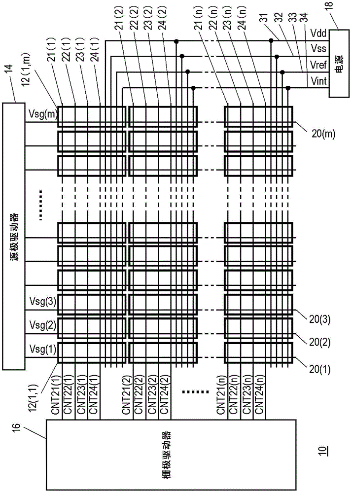
[0028] figure 1 It is a schematic diagram showing the configuration of the image display device 10 in the first embodiment. The image display device 10 in this embodiment has a plurality of pixel circuits 12 (i, j) arranged in a matrix of n rows and m columns (where: 1≤i≤n, 1≤j≤m.), source A driving circuit 14 , a gate driving circuit 16 and a power supply circuit 18 .

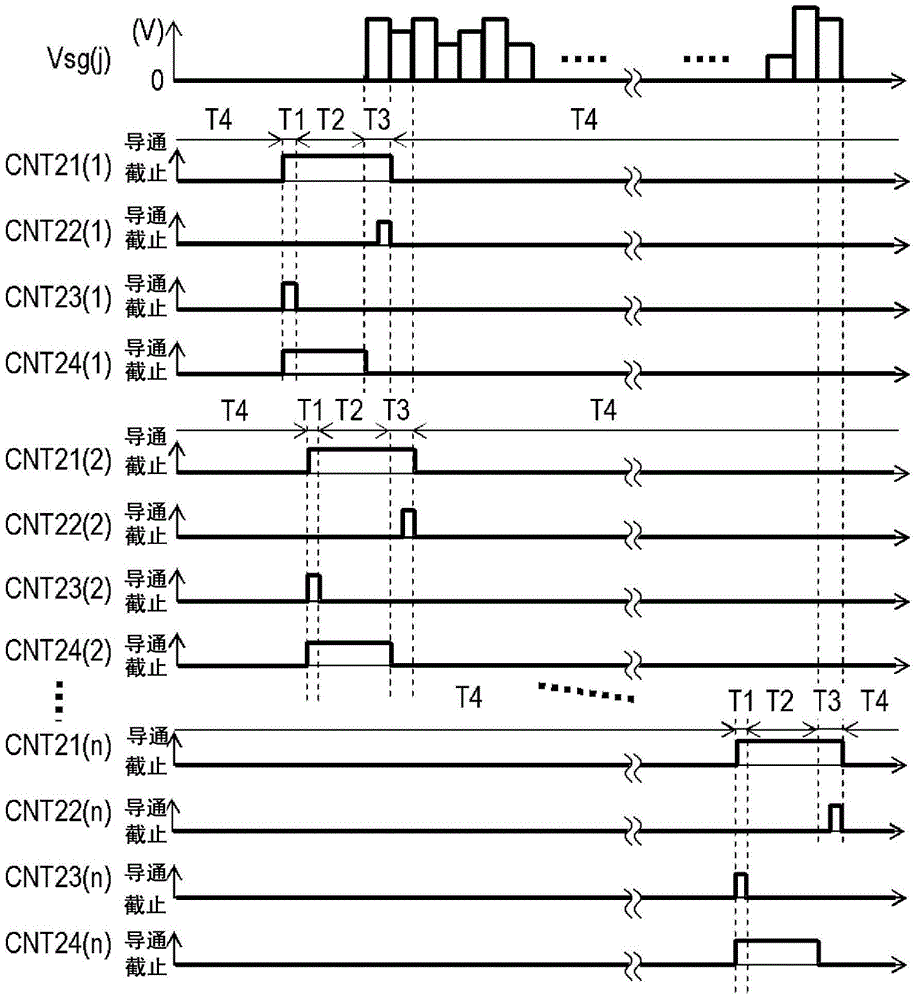
[0029] source drive circuit 14 to figure 1 The data lines 20(j) to which the pixel circuits 12(1,j) to 12(n,j) arranged in the column direction are commonly connected provide the image signal voltage Vsg(j) independently. In addition, the gate drive circuit 16 to figure 1 The control signal lines 21(i)-24(i) connected to the pixel circuits 12(i, 1)-12(i, m) arranged in the row direction provide control signals CNT21(i)-CNT24(i) respectively. . In the present embodiment, four types of control signals CNT21(i) to CNT24(i) are supplied to one pixel circuit 12(i, j), but the number of control signals is not l...

Embodiment approach 2

[0067] Image display device 10 in Embodiment 2 and figure 1 Embodiment 1 shown in has the same structure. Embodiment 2 differs from Embodiment 1 in the configuration of pixel circuits 12 (i, j).

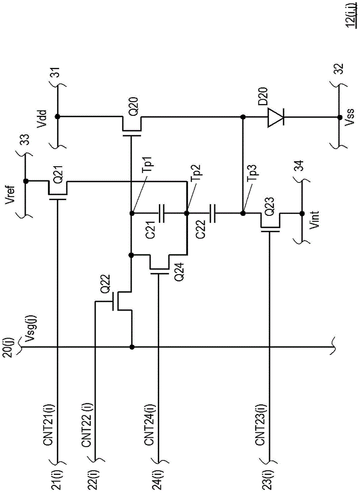
[0068] Figure 9It is a circuit diagram of the pixel circuit 12 (i, j) of the image display device 10 in Embodiment 2. Components that are the same as those in Embodiment 1 are given the same symbols as in Embodiment 1, and detailed description thereof will be omitted. Similar to the first embodiment, the pixel circuit 12 (i, j) in the second embodiment includes an organic EL element D20, a drive transistor Q20, a first capacitor C21, a second capacitor C22, a transistor Q21 that operates as a switch, and a transistor Q22, transistor Q23.

[0069] However, in Embodiment 2, instead of the transistor Q24 which is the fourth switch which short-circuits between the node Tp2 and the gate of the drive transistor Q20, a transistor which is the fourth switch which applies the reference v...

Embodiment approach 3

[0088] Image display device 10 in Embodiment 3 and figure 1 Embodiment 1 shown in has the same structure. Embodiment 3 differs from Embodiment 1 in the configuration of pixel circuits 12 (i, j).

[0089] Figure 10 It is a circuit diagram of the pixel circuit 12 (i, j) of the image display device 10 in the third embodiment. Components that are the same as those in Embodiment 1 are assigned the same reference numerals as in Embodiment 1, and detailed description thereof will be omitted. Like the first embodiment, the pixel circuit 12 (i, j) in Embodiment 3 also has: an organic EL element D20, a drive transistor Q20, a first capacitor C21, a second capacitor C22, and transistors Q21 to Q21 that operate as switches. Q24.

[0090] In Embodiment 3, a transistor Q45 is provided between the source side of the driving transistor Q20 and the organic EL element D20 as a current light emitting element, and this transistor Q45 functions as a fifth switch for cutting off the current fl...


PUM


Abstract

In the image display device of the present invention, a plurality of pixel circuits (12)(i,j) having current light-emitting elements and drive transistors (Q20) passing current to the current light-emitting elements are arranged. The pixel circuit (12) (i, j) is provided with: a first capacitor (C21) with one terminal connected to the gate of the drive transistor (Q20); the other terminal connected to the first capacitor (C21) and the drive transistor The second capacitor (C22) between the sources of (Q20); the first switch (Q21) that applies the reference voltage Vref to the node of the first capacitor (C21) and the second capacitor (C22); to the drive transistor (Q20) The gate of the second switch (Q22) supplies the image signal voltage Vsg; and the third switch (Q23) supplies the initialization voltage Vint to the source of the driving transistor (Q20).

Description

technical field [0001] The present invention relates to an active matrix image display device using a current light emitting element. Background technique [0002] An organic EL display device in which a plurality of self-luminous organic electroluminescent (hereinafter referred to as "organic EL") elements is arranged is considered as a next-generation image display device because it does not require a backlight and has no limitation on the viewing angle. Advance development. [0003] An organic EL element is a current light-emitting element whose brightness is controlled by the amount of current flowing through it. As a method for driving an organic EL element, there are a passive matrix method and an active matrix method. Although the former has a simple pixel circuit, it is difficult to realize a large-scale and high-definition display. Therefore, an active-matrix organic EL display device in which driving transistors are arranged in each pixel circuit has gradually b...

Claims


Application Information

Patent Timeline
Patent Type & Authority Patents(China)
IPC IPC(8): G09G3/30G09G3/20H01L51/50
CPCG09G3/3233G09G3/3291G09G2300/0819G09G2300/0852G09G2300/0861G09G2310/0262G09G2310/067G09G2320/043G09G2320/045G09G3/20G09G3/30
Inventor 柘植仁志
Owner JOLED INC
Why Eureka
Try Eureka