Nonvolatile semiconductor memory

一种非易失性、半导体的技术,应用在半导体器件、半导体/固态器件制造、电固体器件等方向,能够解决有效功函数控制困难等问题

Inactive Publication Date: 2009-07-01
KK TOSHIBA
View PDF1 Cites 0 Cited by
  • Summary
  • Abstract
  • Description
  • Claims
  • Application Information

AI Technical Summary

Problems solved by technology

[0009] In the case of using the technique disclosed in Patent Document 1, it is extremely important to control the effective work function to an optimum value due to (1) the work function of the metal is fixed and (2) the energy band width of the metal is wide. difficult

Method used


Image

  • Nonvolatile semiconductor memory
  • Nonvolatile semiconductor memory
  • Nonvolatile semiconductor memory

Examples


no. 1 example

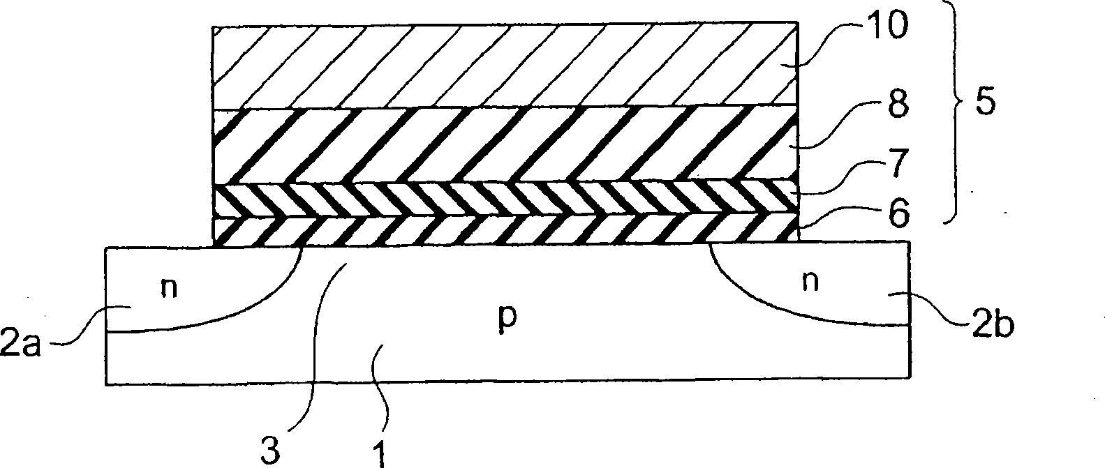
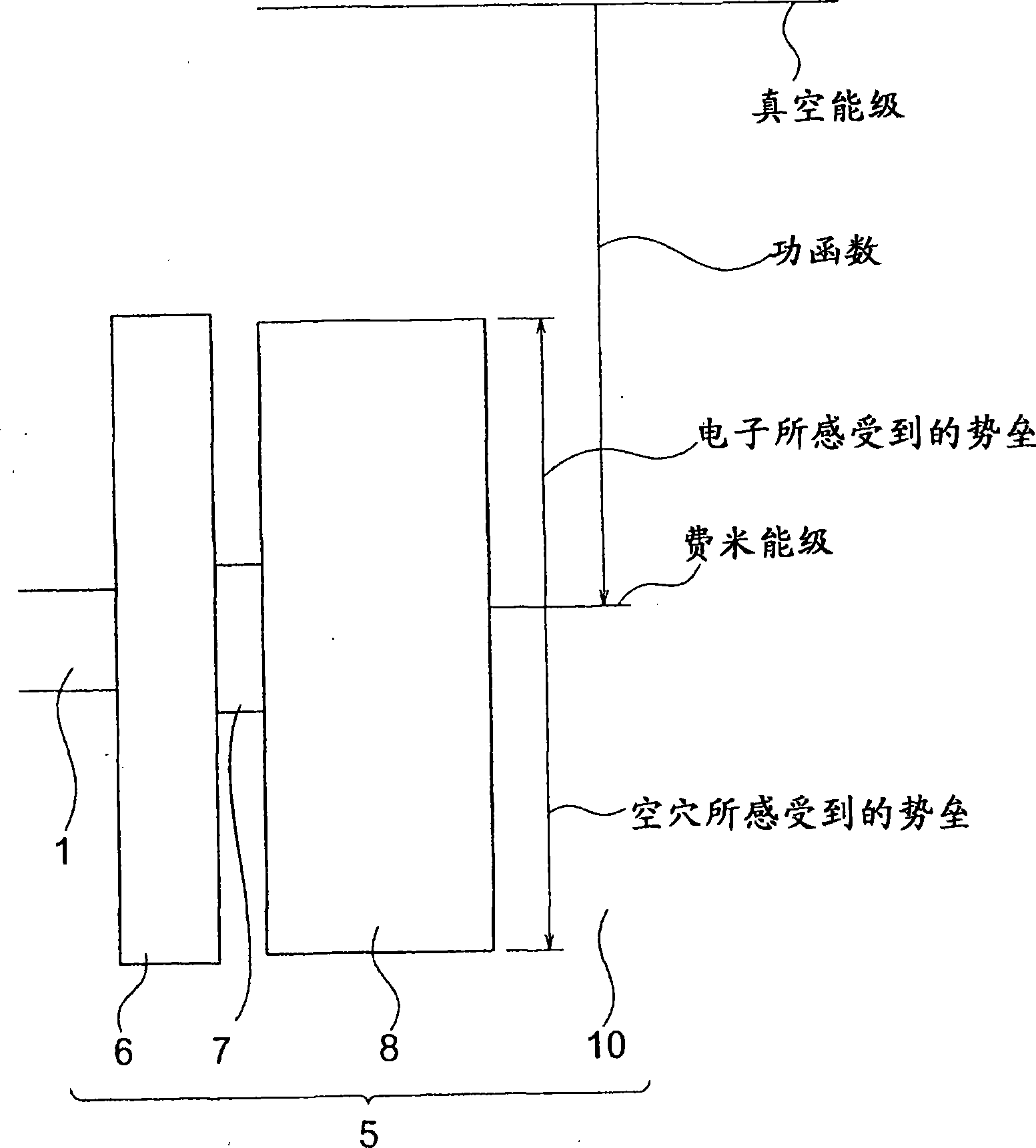
[0077] Next, refer to figure 1 A nonvolatile semiconductor memory according to a first embodiment of the present invention will be described. The nonvolatile semiconductor memory of this embodiment has a plurality of memory cells arranged in a matrix. figure 1 A cross section of each memory cell is shown. In each storage unit, such as figure 1 As shown, an n-type source region 2 a and an n-type drain region 2 b are separately formed in a p-type silicon substrate 1 . The region of the silicon substrate between the source region 2a and the drain region 2b becomes the channel region 3 as a current path. On the channel region 3, a gate 5 for controlling the operation of the memory is provided. The gate 5 has a stacked structure in which a tunnel insulating film 6 , a charge accumulation film 7 , a charge blocking film 8 , and a control electrode 10 are sequentially stacked on the channel region 3 . figure 2 The energy band structure of this gate 5 is shown.

[0078] Next, e...

no. 2 example

[0099] Next, refer to Figure 14 A nonvolatile semiconductor memory according to a second embodiment of the present invention will be described. The nonvolatile semiconductor memory of this embodiment has a plurality of memory cells arranged in a matrix. Figure 14 A cross section of each memory cell is shown. In addition to the control electrode, the memory cell of this embodiment has the same figure 1 The memory cells of the first embodiment shown have exactly the same structure. That is, the storage unit of this embodiment, such as Figure 14 As shown, an n-type source region 2 a and an n-type drain region 2 b are separately formed in a p-type silicon substrate 1 . The region of the silicon substrate between the source region 2a and the drain region 2b becomes the channel region 3 as a current path. On the channel region 3, a gate 5C for controlling the operation of the memory is provided. Gate 5C has a stacked structure in which tunnel insulating film 6 , charge accu...

no. 3 example

[0114] Next, refer to Figure 17 A nonvolatile semiconductor memory according to a third embodiment of the present invention will be described. The nonvolatile semiconductor memory of this embodiment has a plurality of memory cells arranged in a matrix. Figure 17 A cross section of each memory cell is shown. In addition to the control electrode, the memory cell of this embodiment has the same figure 1 The memory cells of the first embodiment shown have exactly the same structure. That is, in the storage unit of this embodiment, as Figure 17 As shown, an n-type source region 2 a and an n-type drain region 2 b are separately formed in a p-type silicon substrate 1 . The region of the silicon substrate between the source region 2a and the drain region 2b becomes the channel region 3 as a current path. On the channel region 3, a gate 5F for controlling the operation of the memory is provided. The gate 5F has a stacked structure in which a tunnel insulating film 6 , a charge...


PUM


Abstract

The present invention provides a nonvolatile semiconductor memory device capable of realizing write-in and erasure at high speed, which includes: a semiconductor substrate; and a memory cell. The memory cell includes: a source region and a drain region formed at a distance from each other on the semiconductor substrate; a tunnel insulating film formed on a channel region of the semiconductor substrate, the channel region being located between the source region and the drain region; a charge storage film formed on the tunnel insulating film; a charge block film formed on the charge storage film; and a control electrode that is formed on the charge block film. The control electrode includes a Hf oxide film or a Zr oxide film having at least one element selected from the first group consisting of V, Cr, Mn, and Tc added thereto, and having at least one element selected from the second group consisting of F, H, and Ta added thereto.

Description

technical field [0001] The present invention relates to a nonvolatile semiconductor memory. Background technique [0002] Generally, flash memory as one of nonvolatile semiconductor memories is a nonvolatile semiconductor memory that does not require an electrical holding operation (holding power supply) for storage, and since programs can be easily written even after the product is completed, So widely used in a variety of electronic equipment. Next-generation and later NAND-type flash memories are required to be further miniaturized and operate at low voltage. [0003] In the memory cell structure of NAND flash memory, for example, a source region and a drain region are formed at intervals in a silicon substrate, and a tunnel insulating film, including A charge trapping film of silicon nitride, a charge blocking film including an insulator, and a stacked structure of a control electrode. In addition, when the above-mentioned charge trapping film is formed of polysilicon...

Claims


Application Information

Patent Timeline
Patent Type & Authority Applications(China)
IPC IPC(8): H01L29/792H01L29/49H01L29/51H01L27/115
CPCH01L29/792H01L21/28282H01L29/513H01L21/28273H01L29/517H01L29/40114H01L29/40117H01L29/66833
Inventor 清水达雄村冈浩一
Owner KK TOSHIBA
Why Eureka
Try Eureka