Electromagnetic conversion device and information memory comprising the same

a technology of information memory and conversion device, applied in the field of information technology, can solve the problems of not being regarded as a true fourth fundamental circuit element, not meaningful, and not satisfying the original definition of memristor, and achieve the effects of infinite times to write, high-speed read and write, and ultra-low power consumption

Active Publication Date: 2018-08-28
INST OF PHYSICS - CHINESE ACAD OF SCI
View PDF29 Cites 0 Cited by
  • Summary
  • Abstract
  • Description
  • Claims
  • Application Information

AI Technical Summary

Benefits of technology

[0019]The electromagnetic conversion device of the present invention realizes the direct conversion between charge and magnetic flux, and thus can be used as the fourth fundamental circuit element, so as to provide a new degree of freedom for the design of electronic circuits and information function devices. In addition, the electromagnetic conversion devices of the present invention comprise transistors and memtransistors depending on the materials of the intermediate magnetoelectric layers. The transistors are formed when the magnetoelectric layers are made of materials having linear magnetoelectric effects. And the memtransistors are formed when the magnetoelectric layers are made of magnetoelectric materials having butterfly-shaped nonlinear hysteresis curves. One of the significant advantages of memtransistors is that a new generation of nonvolatile memory can be implemented with very low power consumption. As the transistors and the memtransistors are composed of insulating magnetoelectric medium, which has a very small internal current as devices, the Joule loss is also very low. Compared with the current-driven resistance-type devices, the transistors and the memtransistors have a great advantage of low power consumption.
[0023]The information memory has the following advantages: (1) high-speed read and write, ultra-low power consumption and infinite times to write; (2) the written data does not lose when power supply is terminated, i.e., it is non-volatile; (3) simple structure, which is beneficial to the realization of large-scale integration and high-density storage. Therefore, it has important applications in the field of information technology.

Problems solved by technology

However, a circuit element M defined by Formula (3) is equivalent to a resistor R, and therefore is not meaningful.
Although the memristor has an important application prospect due to its non-linear memory function, it cannot be regarded as a true fourth fundamental circuit element.
Firstly, the memristor does not satisfy the original definition of the fourth fundamental element (Formula (1)).
Secondly, the memristor is essentially a resistance device, with the operation and action thereof being completely independent of the magnetic flux, and having no magnetic flux memory function.
Thirdly, the memristor as a non-linear device is unequal in status to the other three linear fundamental elements, resulting contradictions in fundamental circuit theories.
Finally, since the memristor is essentially a resistance device, which has a high operation power consumption and is very different from ideal charge-magnetic flux conversion devices with low power consumption, the application thereof is very limited.

Method used


Image

  • Electromagnetic conversion device and information memory comprising the same
  • Electromagnetic conversion device and information memory comprising the same
  • Electromagnetic conversion device and information memory comprising the same

Examples


first embodiment

The First Embodiment

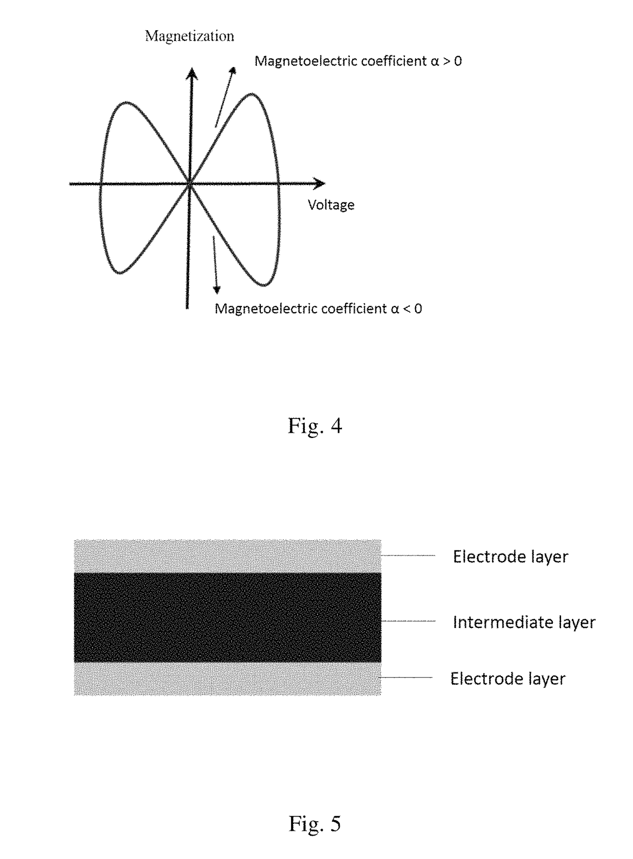
[0061]FIG. 5 shows the structure of a linear transistor according to the present invention, comprising: an intermediate single-crystal BaSrCoZnFe11AlO22 layer and Ag electrode layers located on both sides of the intermediate single-crystal BaSrCoZnFe11AlO22 layer. The single-crystal BaSrCoZnFe11AlO22 layer is a sheet layer with a length, a width and a thickness of 2 mm, 2 mm and 0.3 mm, and with the large surface being (001) plane. The changing of electric polarization ΔP as a function of applied magnetic field H of the linear transistor device of this embodiment is characterized by magnetoelectric current measurements, which are carried out in a Physical Property Measurement System (PPMS), manufactured by Quantum Design Inc., wherein, the measuring temperature is 100 K and the magnetic field H is swept from −100 Oe to 200 Oe continuously. The magnetoelectric current is measured by the Keithley 6517B electrometer and the change of polarization is obtained by inte...

second embodiment

The Second Embodiment

[0062]The structure of a nonlinear memtransistor according to the second embodiment of the present invention is similar to that of the linear transistor of the first embodiment, but with a difference that the intermediate layer is a single-crystal CaBaCo4O7 layer. The single-crystal CaBaCo4O7 layer is a sheet layer with the length, width and thickness of 2 mm, 1 mm and 0.4 mm, respectively, and with the large surface being (001) plane. The changing of electric polarization ΔP as a function of applied magnetic field H of the nonlinear memtransistor of this embodiment is characterized by the magnetoelectric current measurements which are carried out in a Physical Property Measurement System (PPMS) manufactured by Quantum Design Inc., wherein, the measuring temperature is 5 K, the scanning magnetic field during the measurement is in the range of −120 kOe˜+120 kOe, and the change in charges at the electrodes on both ends is measured by the Keithley 6517B electromete...

third embodiment

The Third Embodiment

[0063]The structure of a nonlinear memtransistor according to the third embodiment of the present invention is similar to that of the linear transistor of the first embodiment, with a difference that the intermediate layer is a single-crystal Ba0.5Sr1.5Co2Fe11AlO22 layer. The single-crystal Ba0.5Sr1.5Co2Fe11AlO22 layer is a sheet layer with the length, width and thickness of 2.36 mm, 2.36 mm and 0.39 mm, respectively, and with the large surface being (001) plane. The changing of electric polarization ΔP as a function of applied magnetic field H of the nonlinear memtransistor of this embodiment is characterized by the magnetoelectric current measurements which are carried out in a Physical Property Measurement System (PPMS) manufactured by Quantum Design Inc., wherein, the measuring temperature is 300 K, the scanning magnetic field during the measurement is in the range of −2000 Oe˜+2000 Oe, and the change in charges at the electrodes on both ends is measured by t...


PUM

PropertyMeasurementUnit
thicknessaaaaaaaaaa
thicknessaaaaaaaaaa
thicknessaaaaaaaaaa

Abstract

The present invention provides an electromagnetic conversion device, comprising: an intermediate layer and electrode layers located on both sides of the intermediate layer, wherein the intermediate layer is a magnetoelectric layer. The electromagnetic conversion device realizes the direct conversion of charge and magnetic flux, and thus can be used as a fourth fundamental circuit element, so as to provide a new degree of freedom for the design of electronic circuits and information function devices. In addition, the electromagnetic conversion device can be used as memory elements to form a nonvolatile magnetoelectric information memory.

Description

CROSS-REFERENCE TO RELATED APPLICATIONS[0001]This application claims priority to Chinese application No. 2015100785406, filed on Feb. 13, 2015, which is hereby incorporated by reference as though fully set forth herein.TECHNICAL FIELD[0002]The present invention belongs to the field of information technology and, more particularly, relates to an electromagnetic conversion device and an information memory comprising the same.BACKGROUND OF THE INVENTION[0003]According to the traditional circuit theories, resistors, capacitors and inductors are three fundamental circuit elements, wherein, the resistors are defined by the current-voltage conversion relationship, the capacitors are defined by the voltage-charge conversion relationship, and the inductors are defined by the current-magnetic flux conversion relationship. In 1971, Leon Chua of the University of California, USA proposed theoretically, based on the concept of symmetry, that there should be a fourth fundamental circuit element, ...

Claims


Application Information

Patent Timeline
Patent Type & Authority Patents(United States)
IPC IPC(8): G11C11/22H01L41/02H01L41/083G11C11/02H01F10/14H01L29/82H01L43/02H01F10/16H01L43/10H01L41/20H01L41/187
CPCH01L43/02G11C11/02G11C11/22H01F10/14H01F10/16H01L43/10H01L41/02H01L41/083H01L41/1871H01L41/1875H01L41/20H01L29/82H10N30/80H10N30/00H10N30/85H10N50/80H10N30/50H10N30/8536H10N30/8548H10N35/85H10N50/85
Inventor SUN, YANGCHAI, YISHENGSHANG, DASHAN
Owner INST OF PHYSICS - CHINESE ACAD OF SCI
Why Eureka
Try Eureka