
A method of forming a capacitor structure, and a silicon etching liquid used in this method

A capacitor structure and etching solution technology, applied in capacitors, capacitor manufacturing, chemical instruments and methods, etc., can solve the problems of corrosion of electrodes or other components, and achieve the effect of responding to changes and extension of application time and improving productivity.

Active Publication Date: 2013-11-20
FUJIFILM CORP
View PDF7 Cites 11 Cited by
  • Summary
  • Abstract
  • Description
  • Claims
  • Application Information

AI Technical Summary

Problems solved by technology

However, there is concern that electrodes or other components may be corroded under the action of such solvents

Method used


Image

  • A method of forming a capacitor structure, and a silicon etching liquid used in this method
  • A method of forming a capacitor structure, and a silicon etching liquid used in this method
  • A method of forming a capacitor structure, and a silicon etching liquid used in this method

Examples


example 1 and comparative example 1

[0088] The ingredients shown in Table 1 below were mixed in the composition (% by mass) shown in the following formulation to prepare an etching solution.

[0089]

[0090] Test wafer: A wafer was provided in which a polycrystalline silicon film with a thickness of 500 nm or an amorphous silicon film with a thickness of 500 nm was formed on single-crystal silicon. The wafer was etched with a sheet type etching instrument (POLOS (trade name), manufactured by SPS-Europe B.V.) under the following conditions, and an evaluation test was performed. A wafer with a diameter of 300nm was used, and the evaluation was done by comparing the etch rates at the circumference of two concentric circles, one of which was centered at the center of the wafer and had a radius of 10mm (measured center etch rate: Rc), Another circle 30 mm from the edge (measured edge etch rate: Re).

[0091] Reagent liquid temperature: 80°C

[0092] Discharge volume: 1L / min

[0093] Wafer rotation speed: 500rp...

example 2 and comparative example 2

[0109] 10% by mass of various solvents shown in Table 2 below, 10% by mass of TMAH and 5% by mass of hydroxylamine were added to prepare reagent liquids, all of which had a pH of 12 or more. Using the etching solution thus prepared, an etching test was performed in the same manner as in Example 1 (the etching rate was measured at 10 mm from the center). In addition, the contact angles of silicon and TiN were measured at room temperature. These results are presented in Table 2 below.

[0110]

[0111] From the above results, it can be seen that the contact angle of the etching solution to which the solvent was added was smaller than that of the etching solution to which no solvent was added, and it was confirmed that the wettability was improved. That is, since the enhancement of wettability is confirmed, it can be presumed that silicon residue is less likely to be generated in the capacitor. Furthermore, the improvement in the removability of such silicon residues brings ...


PUM

PropertyMeasurementUnit
thicknessaaaaaaaaaa

Abstract

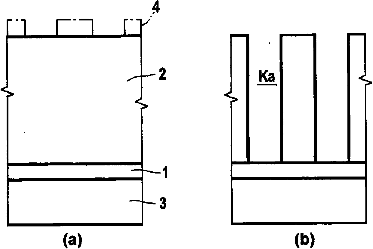
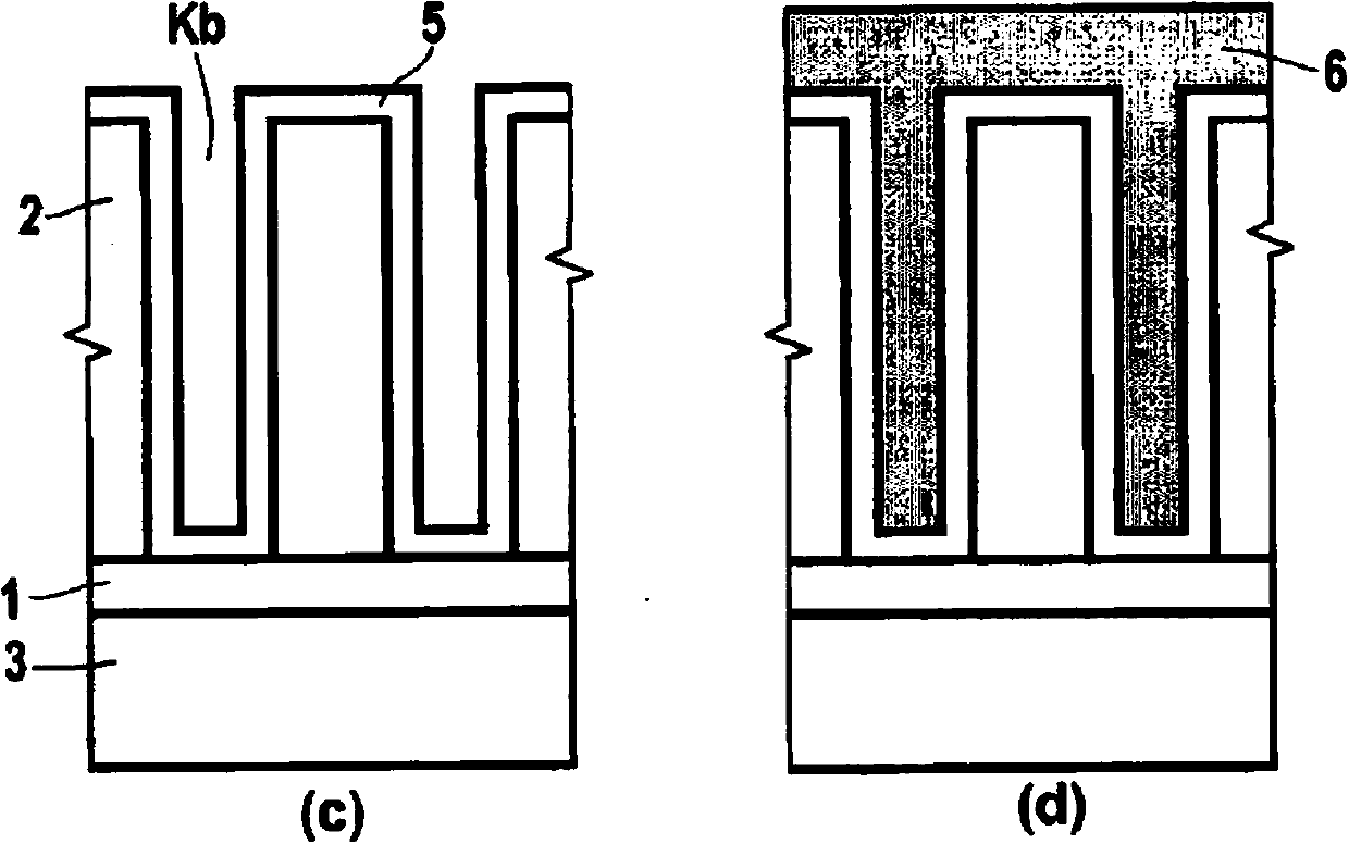
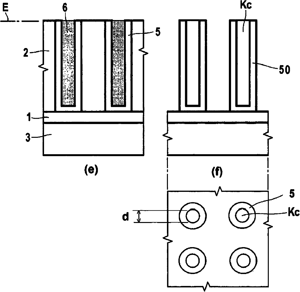
A method of forming a capacitor structure, which comprises: applying a silicon etching liquid which contains an alkali compound and a hydroxylamine compound in combination, with the pH adjusted to 11 or more, to a polycrystalline silicon film or an amorphous silicon film, removing a part or all of the polycrystalline silicon film or amorphous silicon film, and forming concave and convex shapes that constitute a capacitor.

Description

technical field [0001] The invention relates to a method for forming a capacitor structure and a silicon etchant used in the method. Background technique [0002] In a dynamic random access memory (DRAM), a concave structure is often used as a capacitor structure. In this structure, the lower electrode film is usually formed in a cylindrical hole, and only the inner surface is used as an electrode. According to this structure, the area occupied by the capacitor does become smaller, but the diameter of the cylindrical hole must also become smaller. On the other hand, it is necessary to secure a capacitance value required for DRAM element operation. In order to meet the above two requirements, the depth of the cylindrical hole is further deepened. Therefore, it is becoming more and more difficult for micro-process technology to handle the fabrication of capacitors. In view of this situation, a crown type capacitor has been proposed. In its cylindrical structure, not only th...

Claims


Application Information

Patent Timeline
Patent Type & Authority Applications(China)
IPC IPC(8): H01L21/308H01L21/306H01L21/8242H01L27/108
CPCH01L21/32134H01L28/92H01G13/00C09K13/00H01L21/02068C09K13/02H01L21/308H01L21/306H10B99/00H10B12/00
Inventor 水谷笃史稻叶正小山朗子
Owner FUJIFILM CORP
Learn More