Detection method for falling-off of in-grid lead wires of enhanced type power MOS (Metal Oxide Semiconductor) devices
A MOS device and detection method technology, which is applied in the field of microelectronics, can solve the problems of long time consumption and large error of measurement results, and achieve the effects of high efficiency, short measurement time consumption and easy operation
- Summary
- Abstract
- Description
- Claims
- Application Information
AI Technical Summary
Problems solved by technology
Method used
Image
Examples
Embodiment Construction
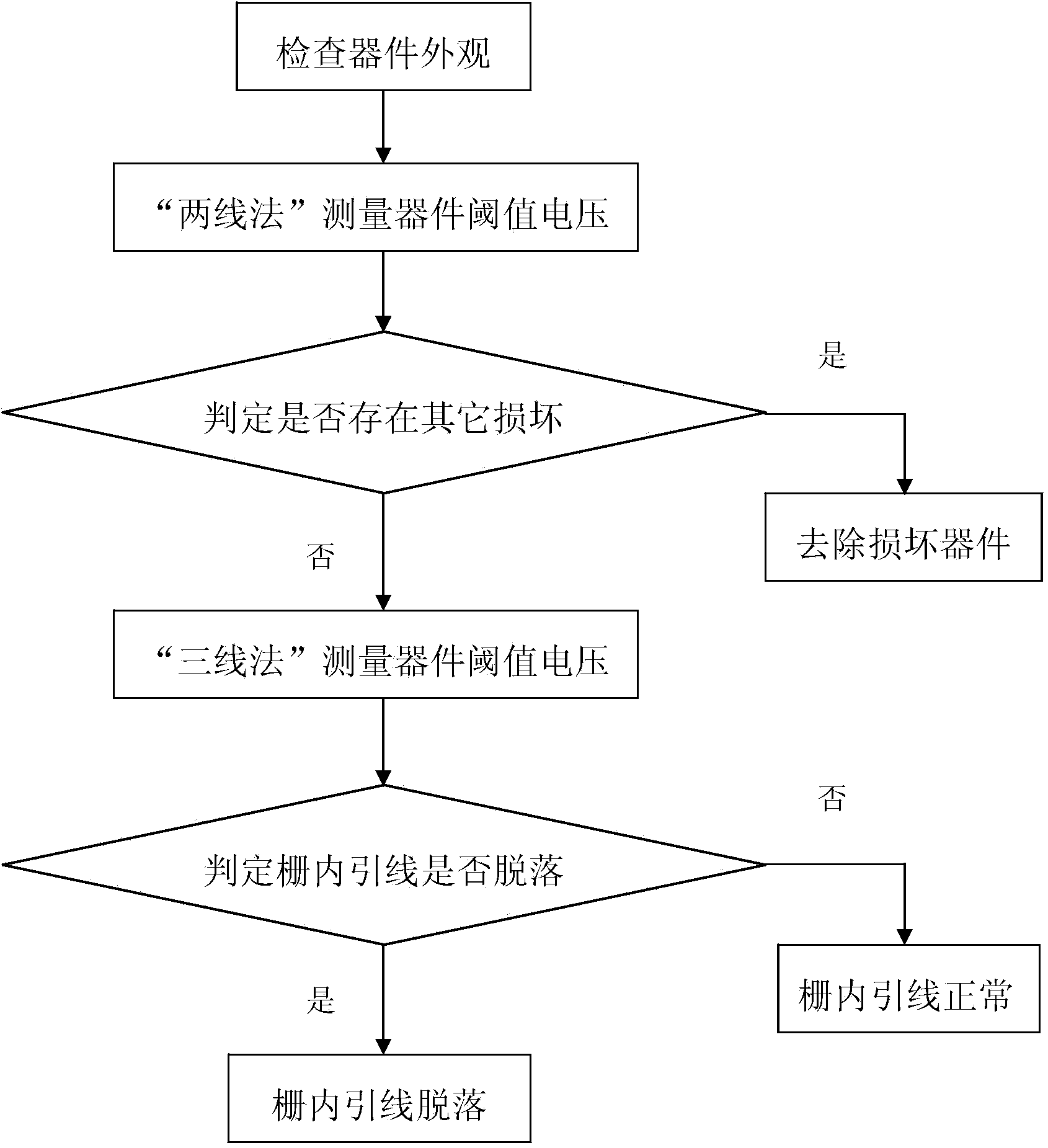
[0023] Attached below figure 1 , to further describe the method of the present invention.
[0024] Step 1, check the appearance of the device.
[0025] Check the appearance of the enhanced power MOS device to be tested, observe whether there is physical damage on the surface of the enhanced power MOS device, remove the enhanced power MOS device with physical damage on the surface, and obtain an enhanced power MOS device with a good surface.
[0026] The physical damage on the surface of the enhanced power MOS device refers to the phenomenon of burn marks on the surface of the device, incomplete pins and leads, or serious deformation of the package. Devices with physical damage on the surface have degraded or even failed in function, and this type of device will interfere with the judgment of lead-off in the gate. Therefore, enhancement mode power MOS devices with physical damage on the surface should be removed.
[0027] Step 2, "two-wire method" to measure the threshold vo...
PUM
 Abstract
Description
Claims
Application Information
 - R&D
- Intellectual Property
- Life Sciences
- Materials
- Tech Scout
- Unparalleled Data Quality
- Higher Quality Content
- 60% Fewer Hallucinations
Browse by: Latest US Patents, China's latest patents, Technical Efficacy Thesaurus, Application Domain, Technology Topic, Popular Technical Reports.
© 2025 PatSnap. All rights reserved.Legal|Privacy policy|Modern Slavery Act Transparency Statement|Sitemap|About US| Contact US: help@patsnap.com

