
Electrostatic discharge detection circuit and processing system

An electrostatic discharge detection and circuit technology, applied in the direction of measuring electricity, measuring devices, measuring electrical variables, etc., can solve the problems of narrow detection range, inability to detect electrostatic voltage, etc., and achieve the effect of improving stability

Active Publication Date: 2016-03-16
GALAXYCORE SHANGHAI
View PDF8 Cites 0 Cited by
  • Summary
  • Abstract
  • Description
  • Claims
  • Application Information

AI Technical Summary

Problems solved by technology

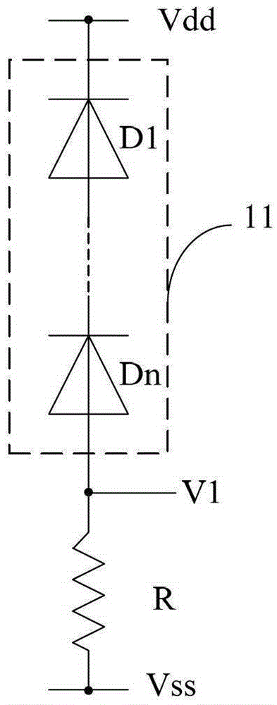
Therefore, the electrostatic discharge detection circuit cannot detect a small electrostatic voltage, and the detection range is narrow

Method used


Image

  • Electrostatic discharge detection circuit and processing system
  • Electrostatic discharge detection circuit and processing system
  • Electrostatic discharge detection circuit and processing system

Examples


Embodiment 1

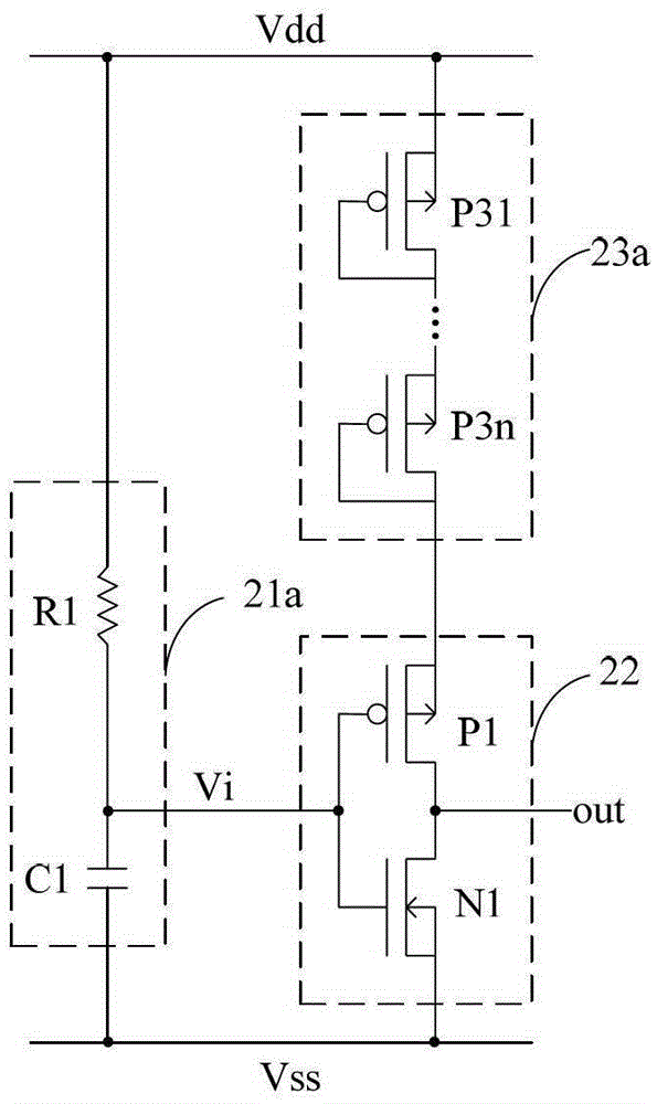
[0049] image 3 is a circuit diagram of an electrostatic discharge detection circuit according to Embodiment 1 of the present invention.

[0050] refer to image 3 , the sampling unit 21a includes a first impedance element R1 and a first capacitive reactance element C1. One end of the first impedance element R1 is connected to the first power supply line Vdd, and the other end of the first impedance element R1 is connected to one end of the first capacitive reactance element C1 and used as the sampling unit 21a to output the control The output terminal of the voltage Vi. The other end of the first capacitive reactance element C1 is connected to the second power line Vss.

[0051] The first impedance element R1 may be composed of various devices including resistors, including polysilicon resistors, active region resistors, well resistors, or MOS channel resistors. The first capacitive reactance element C1 may be composed of capacitors, including polysilicon-insulator-polysi...

Embodiment 2

[0067] Figure 4 is a circuit diagram of an electrostatic discharge detection circuit according to Embodiment 2 of the present invention. refer to Figure 4 , the difference between Embodiment 2 and Embodiment 1 is that the sampling unit 21b includes the first impedance element R1 and the first capacitive reactance element C1, and also includes a second impedance element R2, and the first capacitive reactance element C1 passes The second impedance element R2 is connected to the first impedance element R1, and the connection end of the first impedance element R1 and the second impedance element R2 is used as the output end of the sampling unit 21b to output the control voltage Vi .

[0068] The second impedance element R2 may be composed of various devices including resistors, including polysilicon resistors, active region resistors, well resistors, or MOS channel resistors.

[0069] In this embodiment, the sampling unit 21b includes the second impedance element R2, the seco...

Embodiment 3

[0071] Figure 5 is a circuit diagram of an electrostatic discharge detection circuit according to Embodiment 3 of the present invention. refer to Figure 5 , the difference between embodiment 3 and embodiment 1 is that: the first impedance element R1 and the first capacitive reactance element C1 exchange positions, that is, one end of the first impedance element R1 is connected to the second power line Vss , the other end of the first impedance element R1 is connected to one end of the first capacitive reactance element C1 and serves as the output end of the sampling unit 21c to output the control voltage Vi, and the other end of the first capacitive reactance element C1 is connected to the Describe the first power line Vdd.

[0072]In this embodiment, when the electrostatic voltage generated by electrostatic discharge does not appear on the first power line Vdd, the control voltage Vi is pulled to a low potential through the first impedance element R1, therefore, the contr...


PUM


Abstract

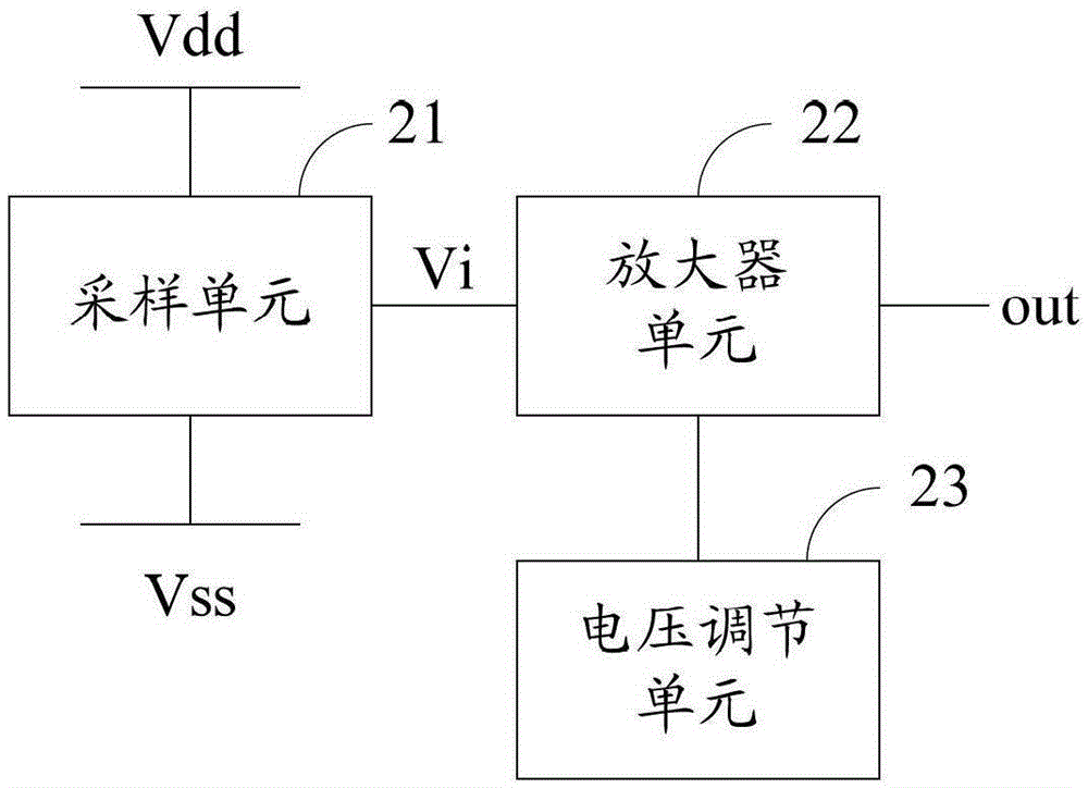
An electrostatic discharge detection circuit and a processing system comprise a sampling unit, an amplifier unit and a voltage adjusting unit, wherein the sampling unit is used for sampling the voltage of a first power wire and the voltage of a second power wire so as to output control voltage, the voltage provided by the first power wire is higher than the voltage provided by the second power wire, the amplifier unit is used for outputting first detection signals when the control voltage is larger than the threshold value voltage of the amplifier unit, and outputting second detection signals when the control voltage is less than the threshold value voltage of the amplifier unit, and the voltage adjusting unit is used for adjusting the threshold value voltage of the amplifier unit. The electrostatic discharge detection circuit can be widened in detection range, and can be used for detection of the inside of a system-level chip with little electrostatic voltage.

Description

technical field [0001] The invention relates to the technical field of electrostatic discharge, in particular to an electrostatic discharge detection circuit and a processing system. Background technique [0002] Electrostatic discharge (ESD, Electro-Static Discharge) is the main factor that causes most electronic components or electronic systems to be damaged by excessive electrical stress. This damage will cause permanent damage to semiconductor devices, resulting in the failure of integrated circuit functions. For system-level chips, the electrostatic voltage generated by electrostatic discharge on the internal power line of the chip is much smaller than the electrostatic voltage at the location where electrostatic discharge occurs. The chip failure caused by electrostatic discharge is the disorder of the logic circuit, rather than directly destroying the internal devices. . Therefore, an electrostatic discharge detection circuit is usually used to detect the electrostat...

Claims


Application Information

Patent Timeline
IPC IPC(8): G01R31/00
Inventor 俞大立陈鑫双赵德林李丽王富中
Owner GALAXYCORE SHANGHAI
Learn More