Power source management driving chip and application circuit thereof

A technology for driving chips and power management, which is applied in the layout of electric lamp circuits, electric light sources, light sources, etc., can solve the problems of inability to use primary side negative feedback, no fixed frequency oscillator, and difficulty in obtaining effective protection, so as to shorten the response time, Cost reduction, high power factor effect

Active Publication Date: 2015-05-20
CHONGQING UNIV OF POSTS & TELECOMM
View PDF3 Cites 0 Cited by
  • Summary
  • Abstract
  • Description
  • Claims
  • Application Information

AI Technical Summary

Problems solved by technology

Although the power factor of the LED drive circuit designed with this chip is high, there is no fixed frequency oscillator inside the chip, and the negative feedback of the primary side cannot be used. Therefore, it is necessary to detect the LED load current, so the drive circuit is more complicated and the cost is higher. like image 3 The schematic diagram of the application circuit based on SN03A is shown
This type of drive circuit has LED open circuit protection and short circuit protection functions, but the short circuit protection needs to provide a detection signal outside the IC, so the response speed is slow, and sometimes it is difficult to effectively protect the LED when the LED is short circuited in actual use.

Method used


Image

  • Power source management driving chip and application circuit thereof
  • Power source management driving chip and application circuit thereof
  • Power source management driving chip and application circuit thereof

Examples


Embodiment Construction

[0045] The specific implementation manner and working principle of the present invention will be further described in detail below in conjunction with the accompanying drawings.

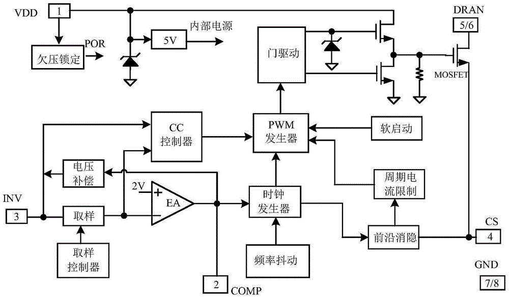
[0046] See Figure 4 , a power management drive chip, which is provided with a power input pin VCC, a ground pin GND, a peak voltage input pin Vmax, a sampling resistor pin Rs, a zero current detection pin ZCD, a current sensing pin CS and a gate driving pin GD, inside the chip It is equipped with V / I converter, delay unit 1, delay unit 2, RS flip-flop, monostable circuit, leading edge blanking circuit, error comparator A1, Schmitt trigger G1, NOT gate G2, follower G3, three-input NAND gate G4, NAND gate G5, NOT gate G6, counter G7, logic control unit G8 and output stage G9, wherein:

[0047] The peak voltage input pin Vmax and the sampling resistor pin Rs are connected to the V / I converter, and the peak voltage signal input by the peak voltage input pin Vmax is converted into a current signal throu...


PUM


Abstract

The invention discloses a power source management driving chip and an application circuit of the power source management driving chip. The chip is provided with a power source input pin, a ground connecting pin, a peak voltage input pin, a sampling resistance pin, a zero current detecting pin, a current inducting pin and a gate driving pin. A V / I converter, a delaying unit 1, a delaying unit 2, an RS trigger, a mono-stability circuit, a leading edge blanking circuit, an error comparator A1, a Schmitt trigger G1, a NOT gate G2, a follower G3, a three-input NAND gate G4, a NAND gate G5, a NOT gate G6, a counter G7, a logic control unit G8 and an output stage G9 are arranged inside the chip. The power source management driving chip has the remarkable advantages that the complexity of the power source driving chip, the physical area and the power dissipation of the chip and the cost of simplification of a driving power source module are reduced, whether a load is an open circuit or a short circuit can be rapidly detected through an internal module of the chip, and the responding time of a control circuit is shortened.

Description

technical field [0001] 本发明涉及集成电路领域,具体地讲,是一种电源管理驱动芯片及该芯片的应用电路。 Background technique [0002] LED是一种符合环保理念的高效绿色光源,在未来十年内将会成为替代传统照明的一大潜力商品。目前市面上针对LED推出的电源管理驱动芯片主要分为两类:第一类是采用原边负反馈、固定开关频率的控制IC,如 figure 1 所示的OB2535芯片结构框图。利用这种芯片设计的LED驱动电路的优点是省略了光耦和用于恒流检测的TL431,因此电路成本较低。但其缺点是功率因素较低(只有0.5~0.6),当LED大量进入百姓家庭时,过低的功率因素会给电网带来非常大的污染。另外,原边反馈虽然可以起到LED负载的开路检测与保护,但不能检测LED短路,因此无法对LED短路做出快速的保护。 [0003] 另一类是具有功率因素校正(PFC)功能的专用驱动芯片,如 figure 2 所示的SN03A芯片结构框图。 这类IC利用芯片内部的模拟乘法器来保证每个开关周期的峰值电流与输入瞬时电压成正比。 虽然采用这种芯片设计的LED驱动电路功率因素高,但其芯片内部没有固定频率的振荡器,无法采用原边负反馈,因此需要检测LED负载电流,故其驱动电路比较复杂,成本较高, Such as image 3 所示的基于SN03A的应用电路原理图。这类驱动电路具有LED的开路保护和短路保护功能,但短路保护需要IC外部提供检测信号,因此响应速度慢,实际运用中有时候在LED短路时难以得到有效保护。 Contents of the invention [0004] 本发明的目的之一是为了提供一种高功率因素且可以通过芯片内部模块快速检测负载是否开路和短路的电源管理驱动芯片,从而缩短控制电路的响应时间,简化芯片的外围电路。 [0005] 为达到上述目的,本发明所采样的技术方案如下: [0006] 一种电源管理驱动芯片,设置有电源输入脚、接地脚,其关键在于:还设置有峰值电压输入脚、采样电阻脚、零电流检测脚、电流感应脚以及栅极驱动脚,在芯片内部设置有V / I变换器、延时单元1、延时单元2、RS触发器、单稳态电路、前沿消隐电路、误差比较器A1、施密特触发器G1、非门G2、跟随器G3、三输入与非门G4...

Claims


Application Information

Patent Timeline
Patent Type & Authority Patents(China)
IPC IPC(8): H05B37/02
Inventor 周前能林金朝李红娟庞宇李章勇李琪李国权蔡雪梅
Owner CHONGQING UNIV OF POSTS & TELECOMM
Why Eureka
Try Eureka