Check patentability & draft patents in minutes with Patsnap Eureka AI!

Switch chip verification method and device based on logic chip

A switch chip and logic chip technology, which is applied in the direction of program control devices, electrical components, transmission systems, etc., can solve the problems of long chip research and development cycle, work overlap, waste of human resources, etc., to shorten the research and development cycle, reduce workload, and facilitate The effect of maintenance

Inactive Publication Date: 2013-12-11
SUZHOU CENTEC COMM CO LTD
View PDF3 Cites 17 Cited by
  • Summary
  • Abstract
  • Description
  • Claims
  • Application Information

AI Technical Summary

Problems solved by technology

[0005] This kind of chip verification method has the following problems: (1) The test cases are designed directly against the chip design specifications, so that in the development process, a large number of test cases need to Corresponding synchronization, and between different chips, because the design structure of the chip changes, it is easy to cause all test cases to be redesigned, and incremental development cannot be done; (2) The test case design must be completed when the chip design and development are completed, and cannot The development of the chip design specification is carried out at the same time, and the development cycle of the chip is long; (3) Although the test cases of the three platforms come from the chip design specification, they still need to maintain their respective test case libraries separately, and there is a large amount of overlap in the work , resulting in a waste of human resources

Method used


Image

  • Switch chip verification method and device based on logic chip
  • Switch chip verification method and device based on logic chip
  • Switch chip verification method and device based on logic chip

Examples


Embodiment Construction

[0024] The technical solutions of the embodiments of the present invention will be clearly and completely described below in conjunction with the accompanying drawings of the present invention.

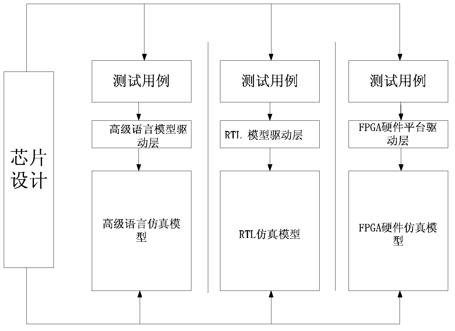
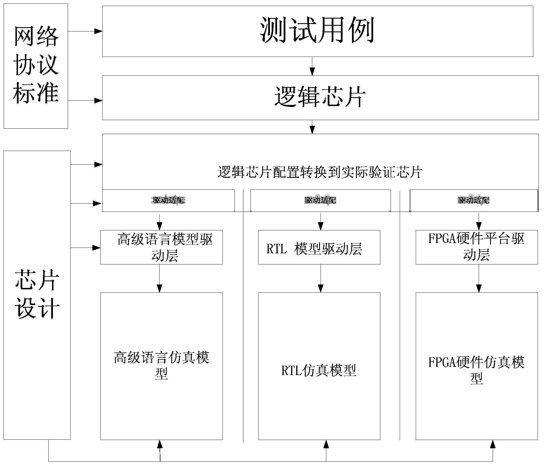
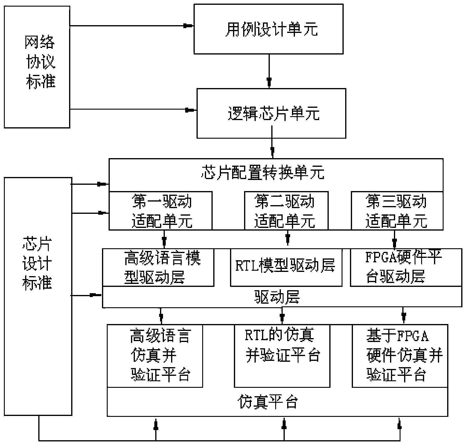
[0025] The invention discloses a verification method for a switch chip based on a logic chip, which is used for verifying the function of the switch chip during the research and development process of the switch chip. Such as figure 2 As shown, the test case completes the configuration of the information required to verify the chip function according to the network protocol standard and the configuration interface information of the logic chip, and sets the test steps for chip verification. The design of the test case in the present invention is directly designed for the logic chip and the network protocol standard, so it is not necessary to wait until the chip design is completed to perform functional verification on the chip, and the design of the test case can be carried out while...


PUM


Abstract

The invention discloses a switch chip verification method based on a logic chip. The switch chip verification method based on the logic chip comprises the steps that a test case is designed according to network protocol standards and the configuration interface information of the logic chip, wherein the configuration information of the test case is stored in the logic chip; a chip configuration conversion module reads the configuration information of the test case from the logic chip and converts the configuration information into configuration information required for verifying the chip; and chip verification is performed based on an independent simulation platform. The invention additionally provides a switch chip verification device based on the logic chip. The switch chip verification device based on the logic chip comprises a case design unit, a chip configuration conversion unit, a logic chip unit and the simulation platform which is connected with the chip configuration conversion unit through a driver layer. The switch chip verification method based on the logic chip and the switch chip verification device based on the logic chip have the advantages that the goal of synchronously performing the design process of the test case and the design process of the chip is realized, the overall research and development period of the chip is shortened, the cost of chip verification and the input of human resources are saved and the chip verification efficiency is improved.

Description

technical field [0001] The invention relates to the field of switch chip verification methods, in particular to a logic chip-based switch chip verification method and device. Background technique [0002] With the rapid development of communication technology, today's switch is no longer a simple message forwarding device, but an intelligent network node that integrates many network protocol standards. In order to adapt to the development of the network, the switch chip is constantly changing Improving the switching capacity and supporting more and more network standards on the other hand will undoubtedly bring a huge workload to the verification of the switch chip in the research and development process. [0003] The R&D investment of a switch chip is large and the cycle is long, and once a switch ASIC chip is put into production, its defects cannot be compensated incrementally. Therefore, in the chip design process, chip verification is very important. During the research...

Claims


Application Information

Patent Timeline
IPC IPC(8): G06F11/36G06F9/455H04L29/06
Inventor 杨曙军
Owner SUZHOU CENTEC COMM CO LTD
Features
  • R&D
  • Intellectual Property
  • Life Sciences
  • Materials
  • Tech Scout
  • Unparalleled Data Quality
  • Higher Quality Content
  • 60% Fewer Hallucinations
Learn More