Optical panel and processing method thereof

A light-transmitting panel, optical technology, applied in the direction of instruments, electrical digital data processing, digital data processing parts, etc., can solve problems such as affecting aesthetics

Inactive Publication Date: 2013-12-18
ASUSTEK COMPUTER INC
View PDF3 Cites 8 Cited by
  • Summary
  • Abstract
  • Description
  • Claims
  • Application Information

AI Technical Summary

Problems solved by technology

However, this design will cause one or several transparent light-transmitting holes on the panel of the notebook computer or tablet computer, so that the user can directly see the sensor or LED light inside the body through the light-transmitting holes, which will affect the operation of the notebook computer or tablet computer. The overall aesthetics of the tablet
However, the conventional manufacturing method of the panel does not make any improvement, that is, one or several light-transmitting holes are left on the panel.

Method used


Image

  • Optical panel and processing method thereof
  • Optical panel and processing method thereof
  • Optical panel and processing method thereof

Examples


Embodiment Construction

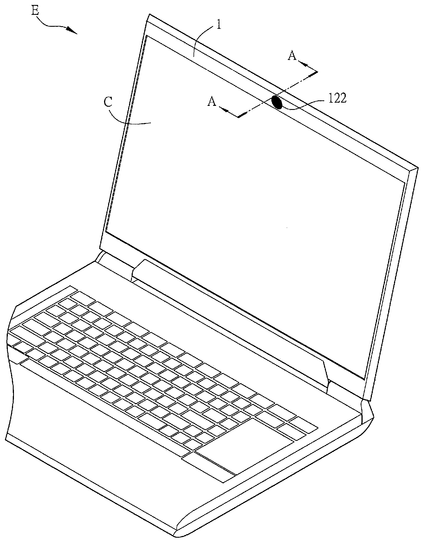
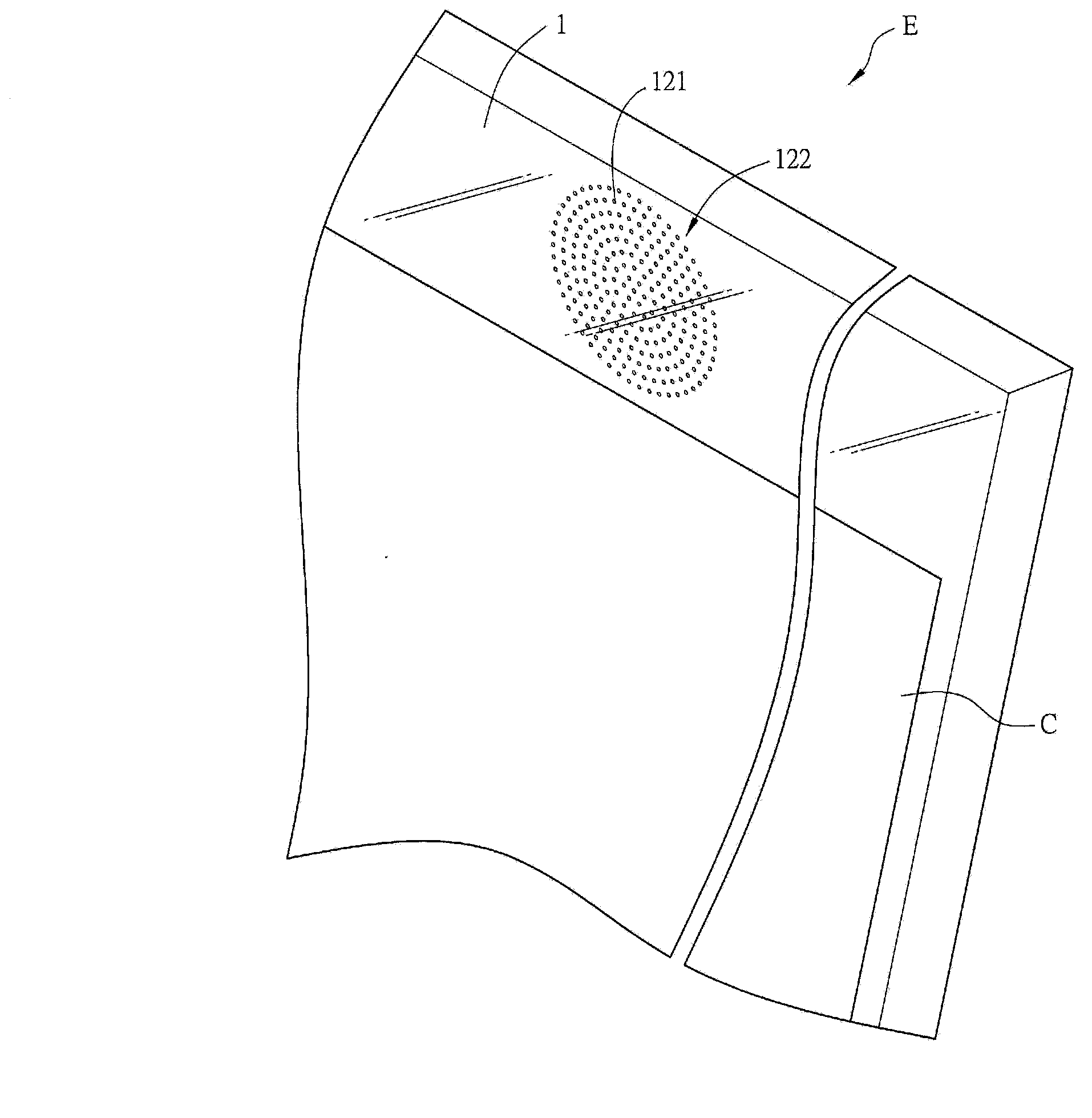
[0016] An optical panel of an electronic device and a manufacturing method thereof according to a preferred embodiment of the present invention will be described below with reference to related drawings, wherein the same components will be described with the same reference symbols.

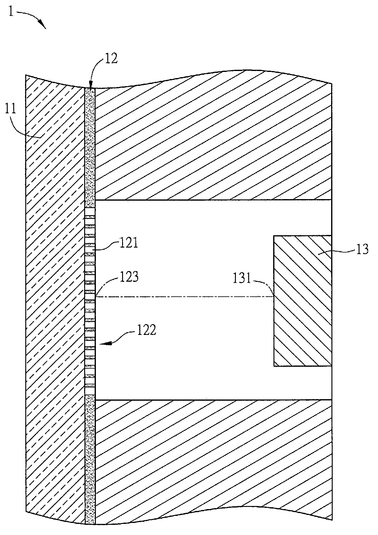
[0017] Figure 1A It is a schematic diagram of an optical panel applied to an electronic device according to an embodiment of the present case, Figure 1B for Figure 1A An enlarged view of a portion of the optical panel shown, figure 2 for Figure 1A The A-A line sectional schematic diagram of the optical panel shown. Such as Figure 1A As shown, an optical panel 1 according to a preferred embodiment of the present invention is mainly applied to an electronic device E. As shown in FIG. In the following, the components and structure of the optical panel 1 will be described first, and then the preparation method of the optical panel 1 will be discussed in detail. Please also refer to Figure 1B...


PUM


Abstract

A processing method of an optical panel used in an electronic device is disclosed. The processing method includes: selecting a light transparent panel and coating a photoresist on one surface of the light transparent panel; forming a plurality of light transmission hole patterns on a photomask; and forming a light shielding layer after the photoresist is exposed via the photomask and developing; and the light transmission hole patterns are transferred to the light shielding layer and a plurality of light transmission holes are formed on the light shielding layer.

Description

technical field [0001] This case relates to an optical panel, in particular to an optical panel used in an electronic device. Background technique [0002] Current electronic devices, especially portable electronic devices, are not only seeking to improve performance and become lighter and thinner, but also tend to develop the overall design and aesthetics of the electronic devices. Take the panels of laptops, tablet computers or smart phones as an example. In order to meet the aesthetic requirements, the frame of the electronic device is formed integrally with the panel without any gaps. , that is, the interior of the electronic device is coated with a layer of ink to conceal the internal structure of the electronic device. [0003] In addition, the current notebook computer or tablet computer will have a built-in light sensor in the panel to sense the light of the external environment, or put an LED (Light Emitting Diode) light or other light sources as a flash unit or in...

Claims


Application Information

Patent Timeline
Patent Type & Authority Applications(China)
IPC IPC(8): G06F1/16
Inventor 陈彦勋骆佑玮黄筱霈洪宗铭
Owner ASUSTEK COMPUTER INC
Why Eureka
Try Eureka