MOS transistor structure and its manufacturing method

A technology of MOS transistor and manufacturing method, applied in the field of MOS transistor structure and its manufacturing, can solve problems such as inability to meet the development requirements of integrated circuits, and achieve the effects of eliminating RDF effect, reducing power consumption, and improving on-current

Active Publication Date: 2015-11-25
SEMICON MFG INT (SHANGHAI) CORP
View PDF5 Cites 0 Cited by
  • Summary
  • Abstract
  • Description
  • Claims
  • Application Information

AI Technical Summary

Problems solved by technology

It can be seen that there is a certain contradiction between the reduction of device size and the reduction of power consumption, which can no longer meet the development requirements of current integrated circuits.

Method used


Image

  • MOS transistor structure and its manufacturing method
  • MOS transistor structure and its manufacturing method
  • MOS transistor structure and its manufacturing method

Examples


Embodiment 1

[0041] Such as Figure 9 As shown, the MOS transistor structure 100 in this embodiment includes:

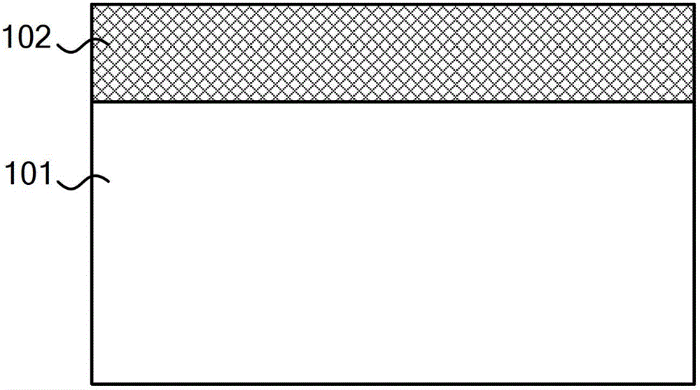
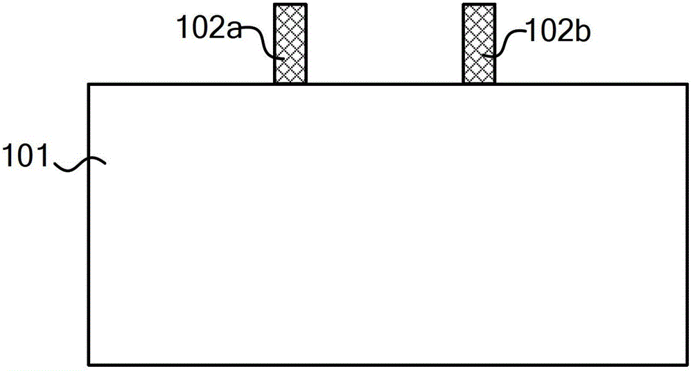
[0042] Substrate 101;

[0043] an isolator formed in the substrate 101, the isolator includes a first isolation block 102a and a second isolation block 102b;

[0044] A lightly doped layer 104 formed on the substrate 101 and the spacer;

[0045] a source region 109 and a drain region 110 formed on both sides of the spacer;

[0046] an undoped layer 105 formed on the lightly doped layer 104;

[0047] a gate structure formed on the undoped layer 105, the gate structure comprising a gate oxide layer 106 and a gate 107; and

[0048] Gate spacers 108 are formed on both sides of the gate structure.

[0049] Wherein, the cross-sectional width of the undoped layer 105 is smaller than or equal to the distance between the first isolation block 102a and the second isolation block 102b, so as to suppress the short channel effect caused by too close source / drain distance.

[0050] Combi...

Embodiment 2

[0061] Such as Figure 16 As shown, the MOS transistor structure 200 in this embodiment includes:

[0062] substrate 201;

[0063] an isolator 202 formed in the substrate 201;

[0064] A lightly doped layer 204 formed on the substrate 201 and the spacer 202;

[0065] a source region 209 and a drain region 210 formed on both sides of the spacer 202;

[0066] an undoped layer 205 formed on the lightly doped layer 204;

[0067] a gate structure formed on the undoped layer 205, the gate structure comprising a gate oxide layer 207 and a gate 208; and

[0068] Gate spacers 209 are formed on both sides of the gate structure.

[0069] Wherein, the cross-sectional width of the undoped layer 205 is smaller than or equal to the cross-sectional width of the spacer 202 .

[0070] Combine below Figure 10 to Figure 16 Each step of the method for manufacturing the MOS transistor structure in Embodiment 2 of the present invention will be described in detail.

[0071] Such as Figure ...

Embodiment 3

[0080] Such as Figure 28 As shown, the MOS transistor structure 300 in this embodiment is the same as the MOS transistor structure 100 in the first embodiment, and will not be repeated here.

[0081] Combine below Figure 17 to Figure 28 Each step of the manufacturing method of the MOS transistor structure according to the third embodiment of the present invention will be described in detail.

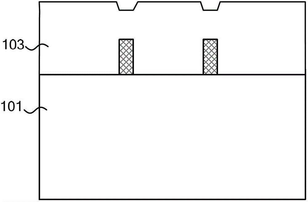
[0082] First, if Figure 17 As shown, a substrate 301 is provided, and a buffer layer film and a mask layer film are sequentially deposited on the substrate 301 . Then etching removes part of the mask layer film, the buffer layer film and part of the thickness of the substrate to form the mask layer 303 and the buffer layer 302 . For the convenience of description, the substrate that has not been etched at all is called the first substrate 301a, the substrate remaining under the mask layer 303 and the buffer layer 302 is called the second substrate 301b, and the mask layer 303 , th...


PUM


Abstract

The invention discloses an MOS transistor structure which comprises a substrate, a separation body formed in the substrate, a light dope layer, a non-dope layer and a grid electrode structure. The light dope layer is arranged on the substrate and the separation body, and the non-dope layer and the grid electrode structure are arranged on the light dope layer. The invention further discloses a manufacturing method of the MOS transistor structure. The method comprises the steps that the substrate is provided, the separation body is formed on the substrate, an epitaxial layer grows on the substrate and the separation body, the first time of ion injection is carried out on the epitaxial layer to form the light dope layer, and the non-dope layer is formed on the light dope layer. According to the technical scheme, contradiction between reduction of the size of the device and power consumption reduction is eliminated.

Description

technical field [0001] The invention belongs to the technical field of integrated circuits, and in particular relates to a MOS transistor structure and a manufacturing method thereof. Background technique [0002] With the wide application of integrated circuits in various portable electronic products. Mobile communications, portable computers and mobile multimedia devices have become one of the products with the highest growth rate, forming a huge market. Their applications are often limited by battery life, and there is little room for improvement in battery life, so power consumption will naturally become an important indicator that needs to be paid attention to in the future development of integrated circuits. At the same time, the integration level of integrated circuits is still increasing gradually, and the device size needs to be further reduced. Smaller size devices are also the goal pursued by integrated circuits in the future. [0003] With the development of su...

Claims


Application Information

Patent Timeline
Patent Type & Authority Patents(China)
IPC IPC(8): H01L29/78H01L29/423H01L21/336H01L21/265
Inventor 刘金华
Owner SEMICON MFG INT (SHANGHAI) CORP
Why Eureka
Try Eureka