
Circuit board, electronic module comprising the same, lighting device, and circuit board manufacturing method

A technology of electronic modules and circuit boards, which is applied to the components of lighting devices, lighting devices, circuit heating devices, etc. It can solve the problems of high thermal resistance of lighting devices, easy breakage or damage of circuit boards, and low thermal conductivity of ceramic substrates.

Inactive Publication Date: 2014-01-15
OSRAM GMBH
View PDF4 Cites 14 Cited by
  • Summary
  • Abstract
  • Description
  • Claims
  • Application Information

AI Technical Summary

Problems solved by technology

This results in a relatively large thermal resistance between the LED chip and the metal base
Taking the relatively new ceramic-based circuit board (Ceramic PCB) as an example, the heat generated by the LED chip, which is also regarded as a heat source, can be transferred to the ceramic through the conductive layer provided on the surface of the ceramic substrate. Substrate, but limited by the characteristics of the ceramic itself, the thermal conductivity of the ceramic substrate is relatively low compared to a metal substrate such as aluminum, so the entire lighting device still has a high thermal resistance
And this kind of ceramic-based circuit board is also easy to break or be broken, and has a large self-weight

Method used


Image

  • Circuit board, electronic module comprising the same, lighting device, and circuit board manufacturing method
  • Circuit board, electronic module comprising the same, lighting device, and circuit board manufacturing method
  • Circuit board, electronic module comprising the same, lighting device, and circuit board manufacturing method

Examples


Embodiment Construction

[0031] In the following detailed description, reference is made to the accompanying drawings which form a part hereof, and in which are shown by way of illustrations specific embodiments in which the invention may be practiced. With respect to the figures, directional terms such as "top", "bottom", "inner", "outer", etc. are used with reference to the orientation of the figures being described. Since components of embodiments of the present invention may be placed in many different orientations, the terminology of orientation is used for illustration only and not in any limiting sense. It is to be understood that other embodiments may be utilized and structural or logical changes may be made without departing from the scope of the present invention. Therefore, the following detailed description should not be taken in a limiting sense, and the invention is defined by the appended claims.

[0032] It should be understood that, unless otherwise specified, features of different e...


PUM


Abstract

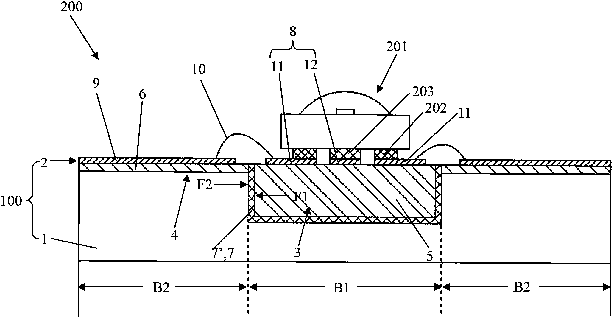
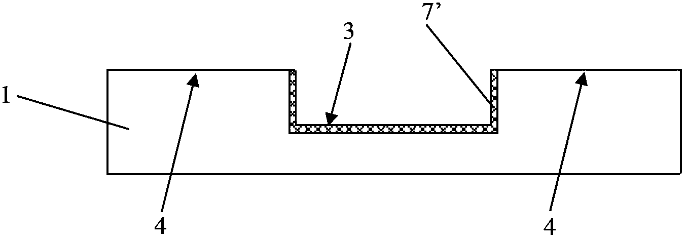
The invention relates to a circuit board (100). The circuit board (100) comprises a substrate (1) and an electrically-conductive layer (2). The circuit board (100) is characterized in that one side of the substrate (1) which is towards the electrically-conductive layer (2) is provided with a first region (3) and a second region (4), wherein the first region (3) is recessed relative to the second region (4), a first insulating layer (5) is accommodated into the first region (3), a second insulating layer (6) is arranged on the second region (4), and the first insulating layer (5) and the second insulating layer(6) have different thermal conductivities. Moreover, the invention further relates to an electronic module comprising the circuit board and a lighting device. The invention further relates to a circuit board manufacturing method.

Description

technical field [0001] The invention relates to a circuit board, an electronic module and a lighting device with the circuit board. Furthermore, the invention relates to a method for producing the circuit board. Background technique [0002] In modern lighting devices, especially high-power LED lighting devices, the thermal resistance of the circuit board accounts for most of the total thermal resistance of the lighting device. Taking the traditional metal-based circuit board (MCPCB) as an example, the heat generated by the LED chip, which can be regarded as a heat source, must pass through the conductive layer and the The insulating layer can be passed to the substrate. Since the insulating layer is usually made of polymer, its thermal conductivity is very low. This results in a relatively large thermal resistance between the LED chip and the metal base. Taking the relatively new ceramic-based circuit board (Ceramic PCB) as an example, the heat generated by the LED chip...

Claims


Application Information

Patent Timeline
IPC IPC(8): H05K1/02H05K1/18H01L33/62H01L33/64F21V23/06F21Y101/02
CPCH05K1/0306H05K1/056H05K1/142H05K2201/09745H05K2201/10106H05K1/0203H05K2201/048H01L2224/48091H01L2224/73265Y10T29/49155H01L2924/00014H05K1/0201H05K1/0204H05K2201/10416H05K1/0284H05K1/053H05K1/181H05K3/10H05K2201/06
Inventor 杨江辉钟传鹏李皓陈小棉
Owner OSRAM GMBH
Learn More