Manufacturing method for forming conductor line on non-conductive substrate

A conductor line and manufacturing method technology, applied in the direction of conductive pattern formation, etc., can solve the problems of high requirements for material control and process technology integration capabilities, high technical threshold, etc., and achieve the effect of reducing material demand, improving bonding strength, and low cost

Inactive Publication Date: 2014-01-22
KUNSHAN LIANTAO ELECTRONICS CO LTD
View PDF6 Cites 8 Cited by
  • Summary
  • Abstract
  • Description
  • Claims
  • Application Information

AI Technical Summary

Problems solved by technology

However, its material control and process technology integration capabilities are relatively high, which makes the technical threshold for entering the DPC industry and stable production relatively high

Method used


Image

  • Manufacturing method for forming conductor line on non-conductive substrate
  • Manufacturing method for forming conductor line on non-conductive substrate
  • Manufacturing method for forming conductor line on non-conductive substrate

Examples


Embodiment Construction

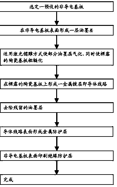
[0023] In order to further have a clearer and more detailed understanding of the purpose, technical solutions and advantages of the present invention, the present invention will be described in detail below in conjunction with the accompanying drawings and specific embodiments.

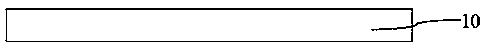
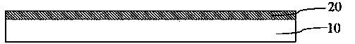
[0024] Please refer to Figure 1 to Figure 7 As shown, the manufacturing method for forming the conductor line 30 on the non-conductive substrate 10 of the present invention includes the following steps:

[0025] a. Select a non-conductive substrate 10, the non-conductive substrate 10 is one of the ceramic materials of alumina, aluminum nitride or silicon carbide, the present invention has no special requirements for the ceramic material of the non-conductive substrate 10.

[0026] b. Form an ink layer 20 on the surface of the non-conductive substrate 10 by spraying, screen printing or roller coating. The ink used in the ink layer 20 is smooth insulating paint with certain elasticity.

[0027] c. Aft...


PUM


Abstract

The invention provides a manufacturing method for forming a conductor line on a non-conductive substrate. The manufacturing method comprises the following steps that: A, a non-conductive substrate is selected; B, a printing ink layer is formed on the surface of the non-conductive substrate; C, laser engraving is performed on the printing ink layer and the surface of the non-conductive substrate through laser, and the laser is utilized to divide the printing ink layer into a plurality of continuous or non-continuous different regional blocks, and then, printing ink layer segments of the non-continuous regional blocks are removed through gasification such that portions of the non-conductive substrate where the non-continuous regional blocks are located are revealed; D, metallization processing is performed on the surfaces of the revealed portions of the non-conductive substrate such that the conductor line which is composed of a metal coating can be formed: D, remaining printing ink layer segments are removed, and the conductor line is formed on the non-conductive substrate.

Description

technical field [0001] The invention relates to a manufacturing method for forming conductor lines on a non-conductive substrate. Background technique [0002] Due to the rapid development of the LED (light-emitting diode) electronics industry, the circuit density on the circuit board is getting higher and higher, resulting in more and more heat accumulated on the circuit board during use, and it is becoming more and more difficult to dissipate. , if the heat energy generated when the LED emits light cannot be exported, the junction temperature of the LED will be too high, which will affect the product life cycle, luminous efficiency, stability, etc. [0003] To improve the luminous efficiency and service life of LEDs, solving the heat dissipation problem of LED products is one of the most important issues at this stage. The development of the LED industry also focuses on high-power, high-brightness, and small-size LED products. Therefore, providing products with High heat ...

Claims


Application Information

Patent Timeline
Patent Type & Authority Applications(China)
IPC IPC(8): H05K3/10
Inventor 李斌汪东平
Owner KUNSHAN LIANTAO ELECTRONICS CO LTD
Why Eureka
Try Eureka