Wire bonding clamp and apparatus and method thereof

A wire bonding and lead technology, applied in the direction of semiconductor devices, electrical components, circuits, etc., can solve the problems of deformation of lead clips, unable to clip leads, bad point shape, etc., so as to increase the force area and reduce the local pressure. oversized effect

Active Publication Date: 2016-05-11
WUXI CHINA RESOURCE MICRO ASSEMBLY TECH
View PDF5 Cites 2 Cited by
  • Summary
  • Abstract
  • Description
  • Claims
  • Application Information

AI Technical Summary

Problems solved by technology

If the clamping force of the lead clamp is too small, it is easy to fail to clamp the lead wire, causing false alarms, resulting in low efficiency, and increasing the workload of employees. If the clamping force of the lead clamp is too large, it is easy to deform the lead clamp, which will eventually lead to quality problems of poor point shape, resulting in poor yield. loss

Method used


Image

  • Wire bonding clamp and apparatus and method thereof
  • Wire bonding clamp and apparatus and method thereof
  • Wire bonding clamp and apparatus and method thereof

Examples


Embodiment Construction

[0030] Reference herein to "one embodiment" or "an embodiment" refers to a particular feature, structure or characteristic that can be included in at least one implementation of the present invention. "In one embodiment" appearing in different places in this specification does not all refer to the same embodiment, nor is it a separate or selective embodiment that is mutually exclusive with other embodiments.

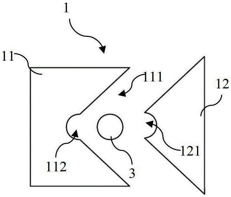
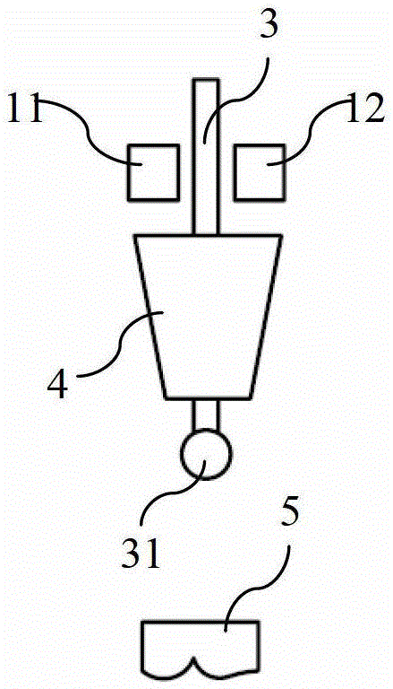
[0031] In the manufacturing process of semiconductor chips, after the wafer is cut into small chips, these exposed chips need to be electrically interconnected with the substrate to realize their electrical functions, and at the same time need to achieve mechanical support and protection. Therefore, these small chips need to be Chips are packaged, wherein different semiconductor chip packaging requirements may be different, and the packaging methods for mounting the chip on the substrate will also be different. The present invention is directed to the packaging equipment ...


PUM


Abstract

The invention provides a jig for wire bonding during semiconductor packaging, and semiconductor packaging equipment and methods using the jig. Wherein the clamp includes a first wire clip and a second wire clip that can hold the lead wire from both sides. Combine, increase the stress area, reduce the lead deformation damage caused by excessive local pressure. At the same time, the first wire clip and the second wire clip use a tapered and tapered matching design, which can realize the limit of the lead wire when the wire clip is opened, and ensure that the lead wire can still be in the depression after the wire clip is opened and closed many times.

Description

【Technical field】 [0001] The invention relates to the field of semiconductor packaging, in particular to the improvement of a lead clamp in a wire bonding packaging mode. 【Background technique】 [0002] In the manufacturing process of semiconductor chips, after the wafer is cut into small chips, these bare chips need to be electrically interconnected with the substrate to realize their electrical functions, and also need to achieve mechanical support and protection. Small chips are packaged. Existing chip packaging methods include wire bonding, automatic tape-carrying technology, and flip-chip technology. [0003] Among them, wire bonding is a process technology that connects the soldering area of ​​the semiconductor chip and the wiring pad on the substrate with a metal filament connector. In the existing wire bonding process, when the wire is bonded, the bonding equipment used usually includes a wire clamp. and chopper. A riving knife is used to stress and cut the leads....

Claims


Application Information

Patent Timeline
Patent Type & Authority Patents(China)
IPC IPC(8): H01L21/68H01L21/687H01L21/60
CPCH01L24/78H01L2224/78301H01L2224/48091H01L2224/48465H01L2924/00014H01L2924/00H01L2224/78621H01L2224/78H01L2924/00012
Inventor 吴俊刘晓明龚平魏元华杨文波
Owner WUXI CHINA RESOURCE MICRO ASSEMBLY TECH
Why Eureka
Try Eureka