CCD chip modulation transfer function test device and method

A modulation transfer function and testing device technology, applied in the field of optical measurement, can solve the problems of good repeatability, discontinuity, and only one or a few pixels can be measured, and achieve simple use, strong versatility, and accurate measurement Effect

Inactive Publication Date: 2014-02-19
XIDIAN UNIV
View PDF4 Cites 28 Cited by
  • Summary
  • Abstract
  • Description
  • Claims
  • Application Information

AI Technical Summary

Problems solved by technology

[0003] In order to solve the need for high-quality optical imaging system and high-precision complex scanning technology to measure the CCD modulation transfer function and the measured modulation transfer function discontinuity in the test process mentioned in the background technology, only one or several images can be measured The weak point of the modulation transfer function of element, the present invention provides a kind of testing device and method of the modulation transfer function of CCD chip that uses frequency-tunable sinusoidal grating as target, device and method of the present invention have wide application range, good repeatability , for easy operation to realize the CCD modulation transfer function

Method used


Image

  • CCD chip modulation transfer function test device and method
  • CCD chip modulation transfer function test device and method
  • CCD chip modulation transfer function test device and method

Examples


Embodiment Construction

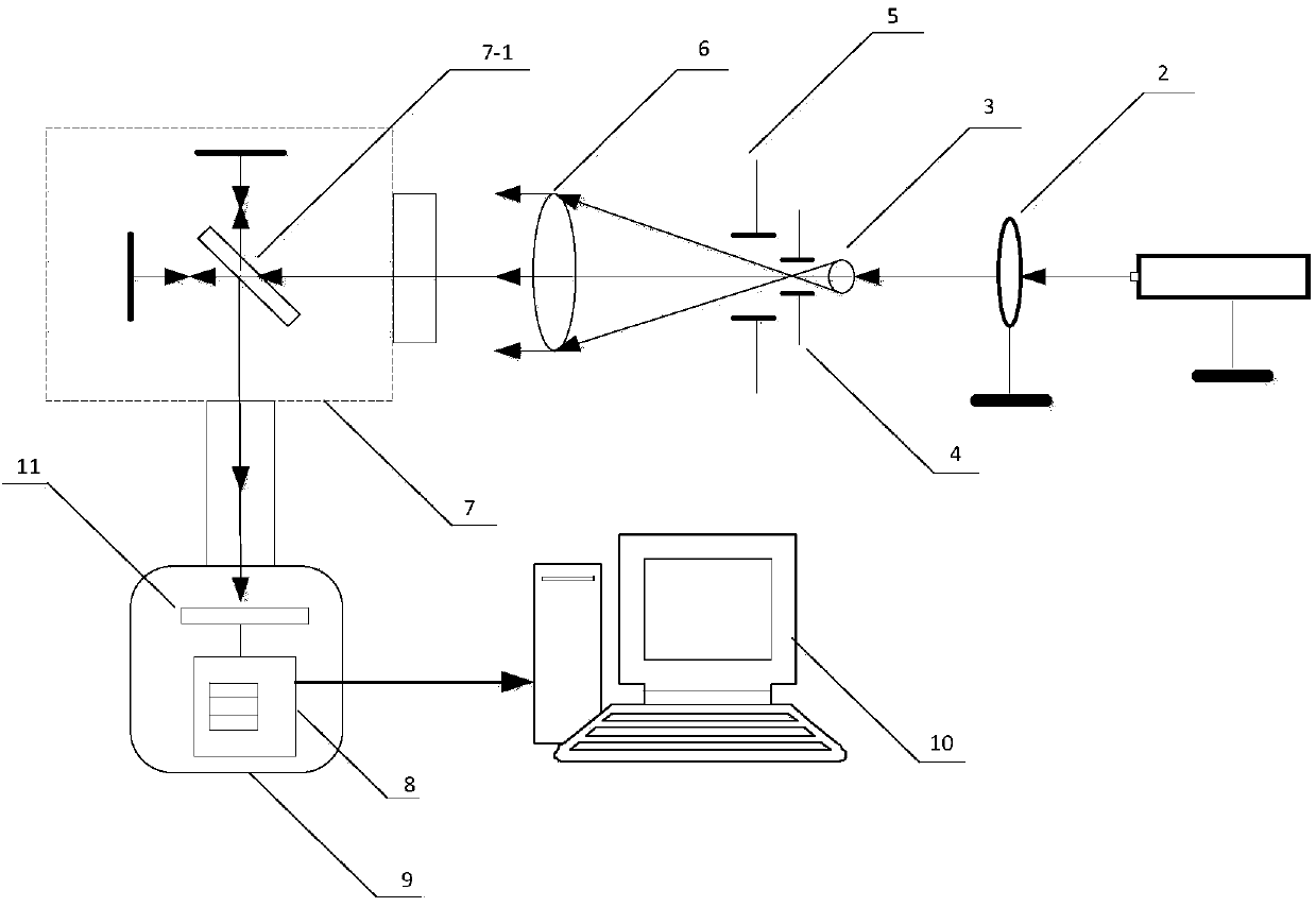
[0022] according to figure 1 , CCD chip modulation transfer function test device includes He-Ne laser 1, adjustable attenuator 2, beam expander 3 pinhole filter 4, aperture 5, collimating lens 6, improved Michelson interferometer 7, image acquisition The card 8, the camera obscura 9, the PC data processing system 10, the CCD chip 11 to be tested, the holographic dry plate and the microphotometer are used in the test, but do not belong to the test device of the present invention. The dark box 9 is placed in the outgoing optical path of the Michelson interferometer 7 and connected through a light-tight pipeline, wherein the CCD chip 11 to be tested is connected with the image acquisition card 8 and arranged in the dark box 9, so as to avoid stray light from affecting the measurement; He-Ne laser 1. The collimating lens 6 and the pinhole filter 4 are sequentially placed on the incident light path of the Michelson interference 7 and the optical axis of each component is on a strai...


PUM


Abstract

The invention discloses a CCD chip modulation transfer function test device and method. The CCD chip modulation transfer function test device mainly comprises a He-Ne laser, an adjustable attenuator, a beam expander, a pinhole filter, a diaphragm, a collimating lens, an improved Michelson interferometer, a camera obscura, an image capture card and a PC data processing system, wherein the He-Ne laser, the adjustable attenuator, the beam expander, the pinhole filter, the diaphragm and the collimating lens are arranged on the incident light path of the improved Michelson interferometer in sequence, and the optical axis of the He-Ne laser, the optical axis of the adjustable attenuator, the optical axis of the beam expander, the optical axis of the pinhole filter, the optical axis of the diaphragm and the optical axis of the collimating lens are arranged on the same straight line, the camera obscura is arranged on the emergent light path of the improved Michelson interferometer, and the PC data processing system is connected with the image capture card which is arranged in the camera obscura and is connected with a CCD. Incident light is processed through the CCD chip modulation transfer function test device to form parallel light, and goes out in a sine interference fringe mode through the improved Michelson interferometer, a sine interference fringe pattern is used as a target, imaging is carried out through the CCD, and a modulation transfer function of the CCD is obtained through a test by using the method of the ratio between the sine interference fringe contrast and the image contrast.

Description

technical field [0001] The invention belongs to the field of optical measurement, and relates to a modulation transfer function test of a CCD chip, in particular to a modulation transfer function test device and method of a CCD chip using a frequency-tunable sinusoidal grating as a target. Background technique [0002] CCD chip is one of the most widely used image sensors in the field of optical imaging, and the demand for evaluating its imaging quality is constantly increasing, and measuring the modulation transfer function is currently recognized as an ideal method for image quality evaluation. At present, there are many measurement devices and methods for MTF, mainly including fixed target measurement MTF method and random target measurement MTF method. In 1977, S.B.Campana first proposed the method of measuring the modulation transfer function of CCD by using point source or detection target. Subsequently, the edge method proposed by S.K.Simonds belongs to the fixed tar...

Claims


Application Information

Patent Timeline
Patent Type & Authority Applications(China)
IPC IPC(8): G01M11/02
Inventor 邵晓鹏高鹏王琳徐军骆秋桦曹蕾程坤
Owner XIDIAN UNIV
Why Eureka
Try Eureka