

A mosfet structure and its manufacturing method
A manufacturing method and stacking technology, applied in semiconductor/solid-state device manufacturing, semiconductor devices, electrical components, etc., can solve problems affecting device performance and other issues
- Summary
- Abstract
- Description
- Claims
- Application Information
AI Technical Summary
Problems solved by technology
Method used
Image

Examples
Embodiment Construction
[0023] In order to make the object, technical solution and advantages of the present invention clearer, the embodiments of the present invention will be described in detail below with reference to the accompanying drawings.
[0024] Embodiments of the present invention are described in detail below, examples of which are shown in the drawings, wherein the same or similar reference numerals designate the same or similar elements or elements having the same or similar functions throughout. The embodiments described below by referring to the figures are exemplary only for explaining the present invention and should not be construed as limiting the present invention.
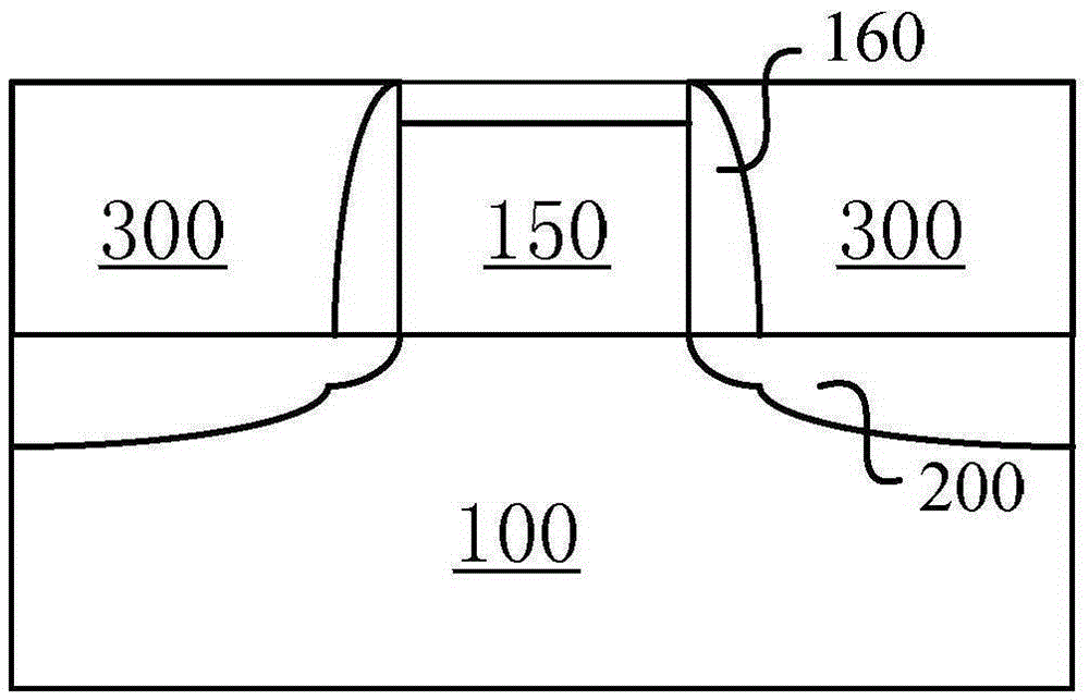
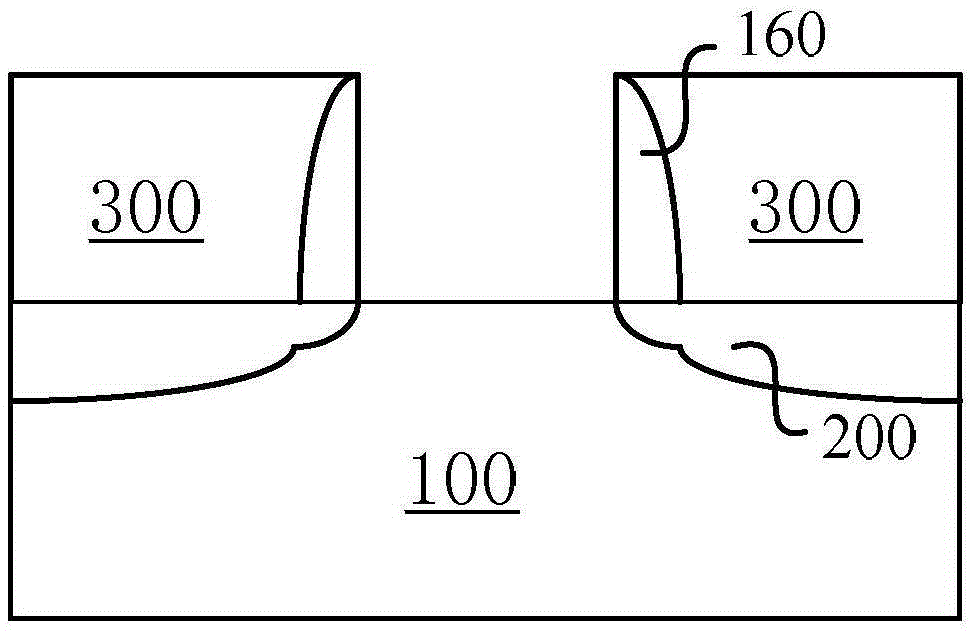
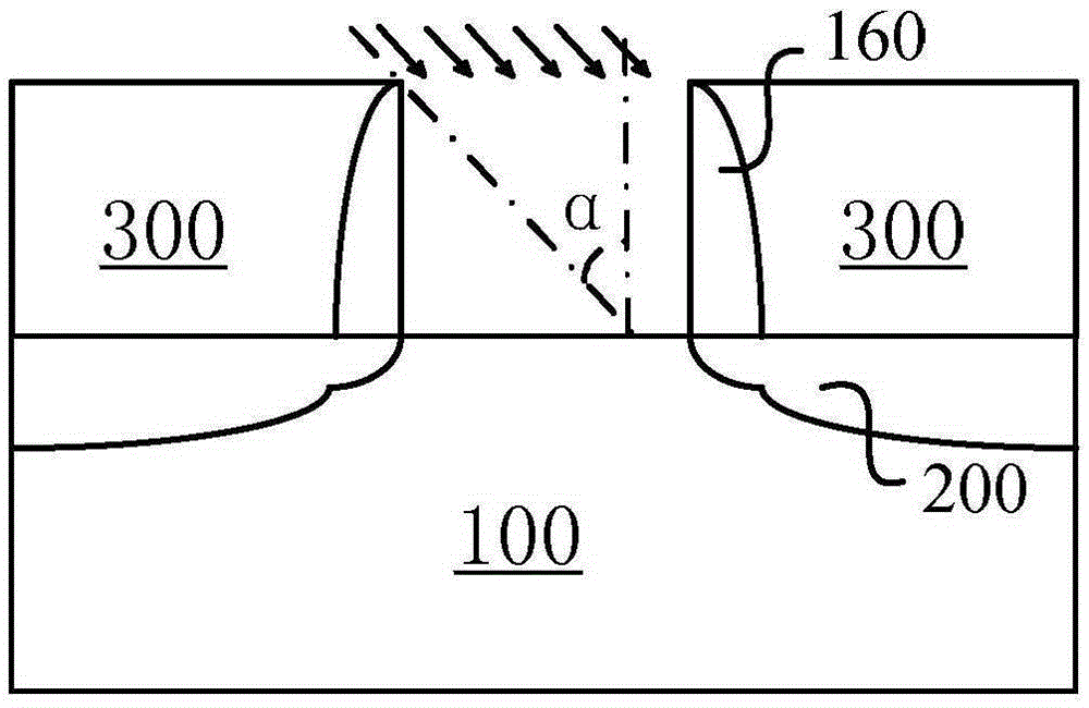
[0025] Such as Figure 5 As shown, the present invention provides an asymmetric MOSFET structure, including: a substrate 100; a gate stack 500 located above the substrate 100; source and drain located in the substrate on both sides of the gate stack 500 region 200; sidewalls 160 on both sides of the gate stack 500;...
PUM
 Abstract
Description
Claims
Application Information