Supercharge Your Innovation With Domain-Expert AI Agents!

Semi-automatic Wafer Ball Mounting Equipment

A semi-automatic, wafer-based technology, applied in the direction of semiconductor devices, semiconductor/solid-state device manufacturing, electrical components, etc., can solve problems such as operational errors, high prices, low efficiency, etc., to ensure accuracy and speed, low maintenance costs, cost reduction effect

Active Publication Date: 2016-01-13
SHANGHAI WEISONG IND AUTOMATION
View PDF4 Cites 0 Cited by
  • Summary
  • Abstract
  • Description
  • Claims
  • Application Information

AI Technical Summary

Problems solved by technology

[0003] 1. Using the human eye to align the position through the display, the accuracy is poor and the efficiency is low, and it is difficult to guarantee the yield
[0004] 2. Wafer loading and unloading is done manually, which is likely to cause operational errors and fragments
[0006] 1. At present, this type of equipment on the market uses multiple CCDs to align the wafer, the printing mechanism and the ball-planting mechanism, resulting in high cost and high price
[0007] 2. The automatic ball planting mechanism is very complicated, the cost is high, and the workload is relatively large when replacing new products

Method used


Image

  • Semi-automatic Wafer Ball Mounting Equipment
  • Semi-automatic Wafer Ball Mounting Equipment

Examples


Embodiment Construction

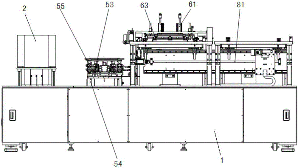
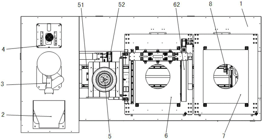
[0021] see figure 1 , figure 2 , the semi-automatic wafer ball planting equipment of the present invention comprises a bottom stand 1, on which a wafer loading / unloading mechanism 2, a wafer transfer manipulator 3, a wafer calibration mechanism 4, a wafer loading platform 5, a wafer Circular printing mechanism 6, wafer ball planting mechanism 7 and CCD alignment system 8. Wafer loading / unloading mechanism 2, wafer transfer manipulator 3 and wafer alignment mechanism 4 are sequentially arranged at one end of bottom stand 1 along the y-axis direction, wafer loading stage 5, wafer printing mechanism 6, wafer ball planting The mechanism 7 and the CCD alignment system 8 are sequentially arranged on the bottom platform along the x-axis direction, and the wafer loading platform 5 is arranged adjacent to the wafer transfer robot 3, and the wafer ball planting mechanism 7 and the CCD alignment system 8 are combined and adjacent A wafer printing mechanism 6 is provided.

[0022] The...


PUM


Abstract

The invention discloses a semi-automatic wafer ball mounting device. The ball mounting device comprises a bottom stand, wherein a wafer charging / discharging mechanism, a wafer conveying mechanical arm, a wafer calibrating mechanism, a wafer carrying table, a wafer printing mechanism, a wafer ball mounting mechanism and a CCD (Charge Coupled Device) aligning system are arranged on the bottom stand. The wafer charging / discharging mechanism, the wafer conveying mechanical arm and the wafer calibrating mechanism are sequentially arranged at one end of the bottom stand along the y-axis direction; the wafer carrying table, the wafer printing mechanism, the wafer ball mounting mechanism and the CCD aligning system are sequentially arranged on the bottom stand along the x-axis direction; the wafer carrying table is arranged near the wafer conveying mechanical arm; the wafer ball mounting mechanism and the CCD aligning system are combined together near the wafer printing mechanism. Through automatic CCD alignment, the accuracy and the rapidness of alignment are guaranteed; the ball mounting device is applicable to different wafers of 6-inch, 8-inch and 12-inch just by means of replacing jigs and carriers.

Description

technical field [0001] The invention relates to semiconductor production equipment, in particular to a semi-automatic wafer ball planting equipment. Background technique [0002] The wafers manufactured in the semiconductor front-end process need to go through the packaging process to become the final chip. Wafer-level packaging has become the mainstream of the market. Wafer-level packaging is being widely used in large-scale integrated circuits due to its advantages of high density, small size, good heat dissipation, and excellent electrical performance. A core process of wafer-level packaging technology is bumping. At present, in terms of wafer ball planting process in China, some of them use manual ball planting table to realize the disadvantages of this manual ball planting method: [0003] 1. Using the human eye to align the display through the display, the accuracy is poor and the efficiency is low, and it is difficult to guarantee the yield. [0004] 2. Wafer loadi...

Claims


Application Information

Patent Timeline
Patent Type & Authority Patents(China)
IPC IPC(8): H01L21/60H01L21/68
CPCH01L21/681H01L24/742H01L2224/742
Inventor 刘劲松毕秋吉钟亮
Owner SHANGHAI WEISONG IND AUTOMATION
Features
  • R&D
  • Intellectual Property
  • Life Sciences
  • Materials
  • Tech Scout
  • Unparalleled Data Quality
  • Higher Quality Content
  • 60% Fewer Hallucinations
Learn More