A polycrystalline silicon resistor and a manufacturing method thereof

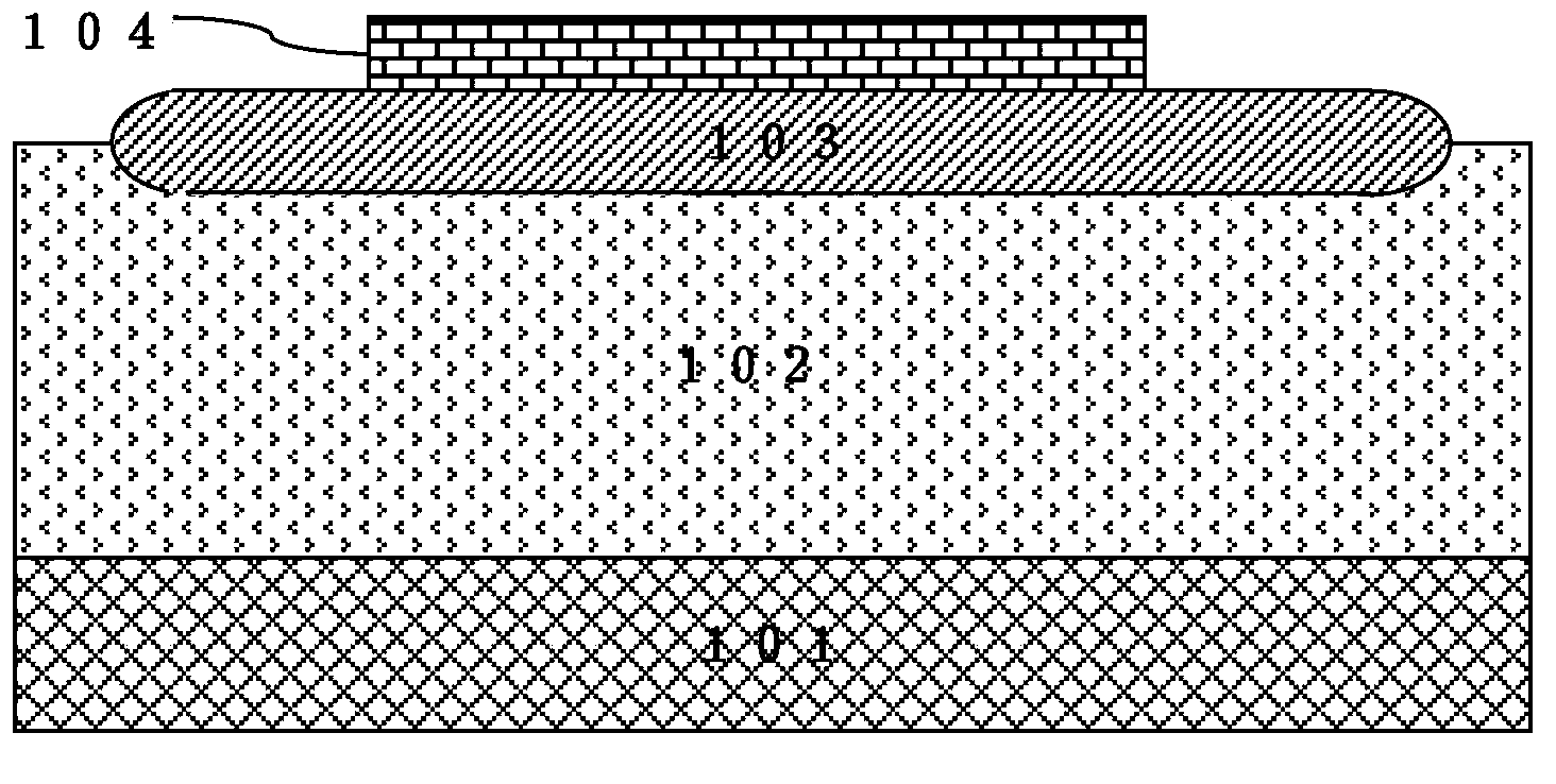
A technology of polysilicon resistors and polysilicon, applied in semiconductor/solid-state device manufacturing, circuits, electrical components, etc., can solve the problems of local field oxide layer 103 breakdown, polysilicon resistors cannot reach high voltage, etc.

Active Publication Date: 2014-03-12
SHANGHAI HUAHONG GRACE SEMICON MFG CORP
View PDF5 Cites 10 Cited by
  • Summary
  • Abstract
  • Description
  • Claims
  • Application Information

AI Technical Summary

Problems solved by technology

However, if the existing polysilicon resistance is applied to a higher operating voltage occasion, the local field oxide layer 103 will be broken down. Assuming that the required operating voltage of the polysilicon resistance 104 is 700V, and the breakdown electric field of the local field oxide layer 103 When it is 1E6V / cm, the thickness of the required local field oxide layer 103 is at least 7 μm, and the local field oxide layer 103 of such thickness is impossible to obtain
The working voltage of existing polysilicon resistors cannot reach high voltages above 700V

Method used


Image

  • A polycrystalline silicon resistor and a manufacturing method thereof
  • A polycrystalline silicon resistor and a manufacturing method thereof
  • A polycrystalline silicon resistor and a manufacturing method thereof

Examples


Embodiment Construction

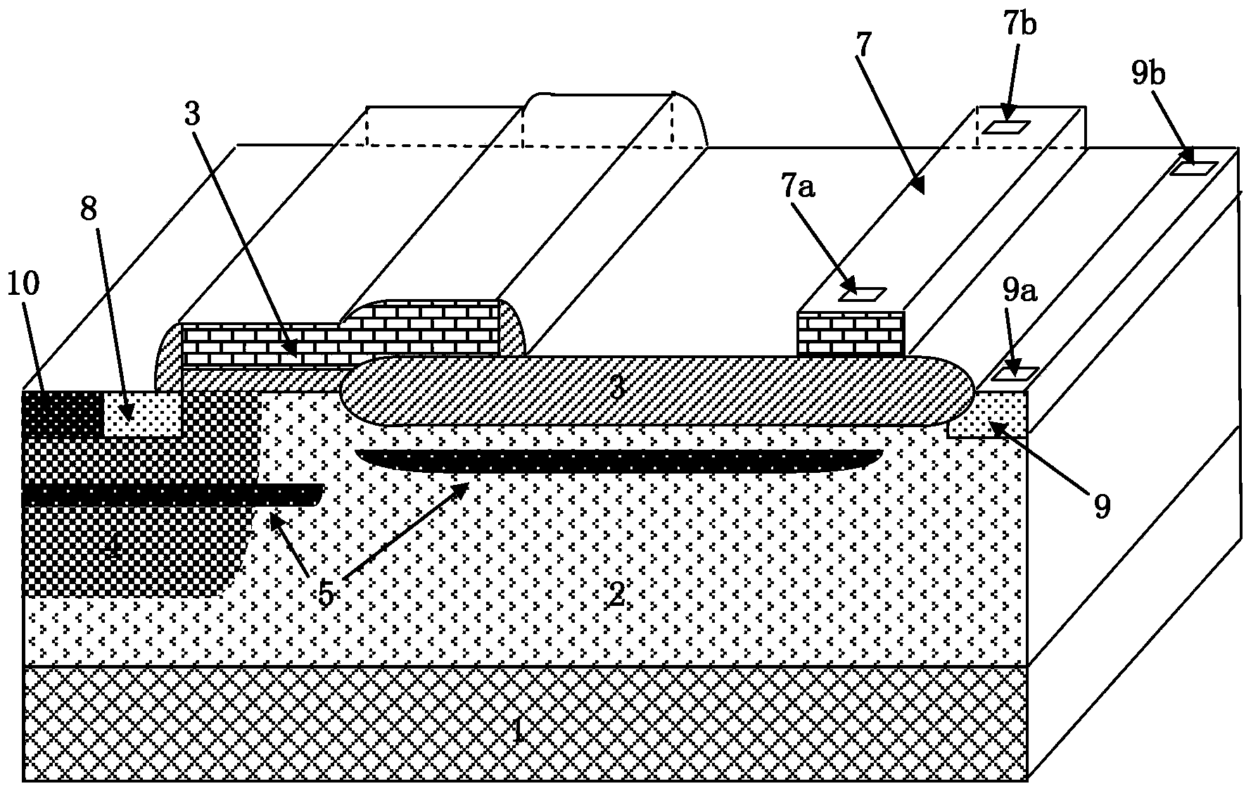
[0043] Such as figure 2 Shown is a schematic structural diagram of a polysilicon resistor according to an embodiment of the present invention. The polysilicon resistor of the embodiment of the present invention, the LDMOS device used in the polysilicon resistor of the embodiment of the present invention is described by taking an N-type LDMOS device as an example. The polysilicon resistor of the embodiment of the present invention includes:

[0044] A P-type silicon substrate 1, an N-type well region 2 is formed on the silicon substrate 1, and a field oxide layer 3 is also formed on the silicon substrate 1. The N-type well region 2 is formed by ion implantation and high-temperature push well before the formation of the field oxide layer 3. The implanted impurity of the ion implantation in the N-type well region 2 is phosphorus, and the implantation energy is 100keV-300keV. dose of 10 11 cm -2 ~10 14 cm -2 , the temperature of the high-temperature push well in the N-type w...


PUM


Abstract

The invention discloses a polycrystalline silicon resistor. A field oxide layer forms on a silicon substrate. The polycrystalline silicon resistor is arranged on the field oxide layer of a drain terminal of an LDMOS device. In a width direction, a first resistor electrode and a second resistor electrode respectively form at the two ends of the polycrystalline silicon resistor. A first drain terminal electrode and a second drain terminal electrode respectively form on positions of a same width at the two ends of a drain region. In a usage process, same voltages are applied to the first drain terminal electrode and the first resistor electrode, and the same voltages are applied to the second drain terminal electrode and the second resistor electrode. The invention also discloses the manufacturing method of the polycrystalline silicon resistor. According to the invention, a working voltage of the polycrystalline silicon resistor can be raised, and the polycrystalline silicon resistor can work at a bias voltage of 700V or to more than 700V.

Description

technical field [0001] The invention relates to the field of semiconductor integrated circuit manufacturing, in particular to a polysilicon resistor. The invention also relates to a method for manufacturing polysilicon resistors. Background technique [0002] Such as figure 1 Shown is a schematic diagram of the structure of an existing polysilicon resistor. The structure of an existing polysilicon resistor includes: a substrate 101; a well region 102 formed on the substrate 101, which can be a P-type well region or an N-type well region; a local field oxidation A layer (LOCOS) 103 is used to isolate an active region on the substrate 101 ; a polysilicon resistor 104 is formed above the local field oxide layer 103 . Existing polysilicon resistors are generally used in occasions where the operating voltage is low. When the operating voltage is low, the thickness of the local field oxide layer 103 can fully withstand the voltage on the polysilicon resistor 104 and the well reg...

Claims


Application Information

Patent Timeline
Patent Type & Authority Applications(China)
IPC IPC(8): H01L27/06H01L21/02
Inventor 董金珠胡君
Owner SHANGHAI HUAHONG GRACE SEMICON MFG CORP
Why Eureka
Try Eureka