TEM sample repreparation method

A technology of sample and sample holder, which is applied in the field of TEM sample re-preparation to achieve the effect of improving the success rate

Active Publication Date: 2014-03-19
SHANGHAI HUALI MICROELECTRONICS CORP
View PDF11 Cites 7 Cited by
  • Summary
  • Abstract
  • Description
  • Claims
  • Application Information

AI Technical Summary

Problems solved by technology

[0011] The method of this patent improves the success rate of sample extraction, but does not re-prepare the sample

Method used


Image

  • TEM sample repreparation method
  • TEM sample repreparation method
  • TEM sample repreparation method

Examples


Embodiment 1

[0052] In this embodiment, the samples that need to be re-prepared are those that are too thick to be observed by TEM.

[0053] The specific re-preparation method is as follows:

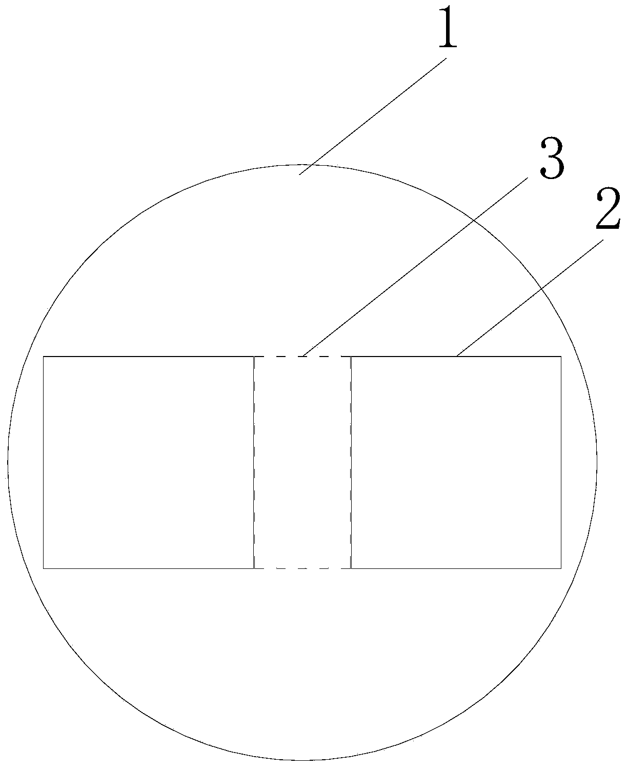
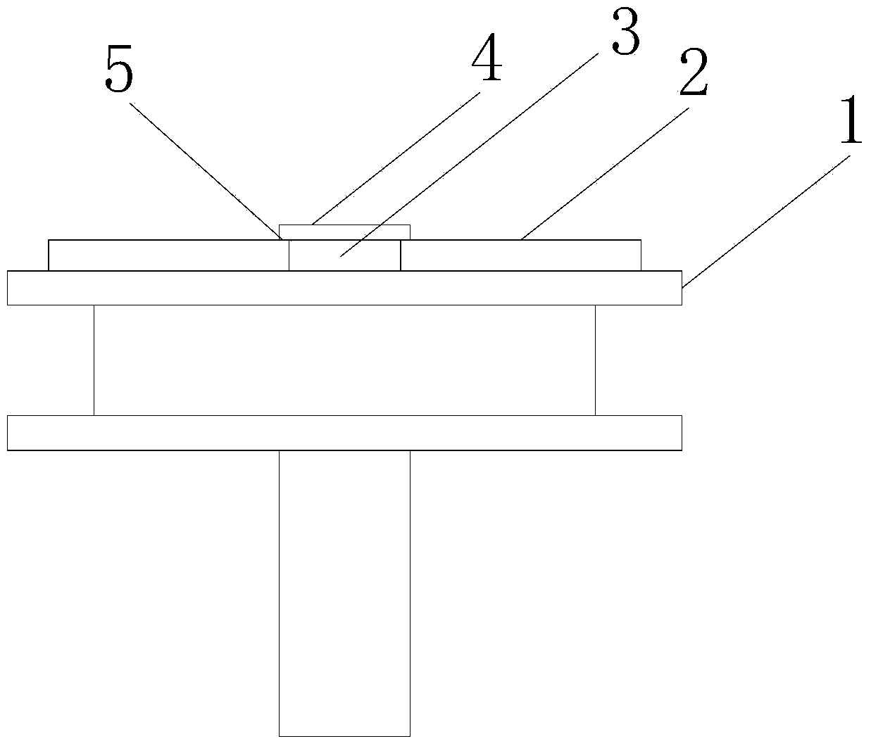
[0054] First, a carbon film copper grid frame with several samples placed on the surface is placed between two small silicon chips attached to the SEM / FIB sample holder, and the part of the carbon film copper grid in contact with the two small silicon chips is coated with There is silver glue to fix the carbon film copper mesh and two small silicon chips. There is a certain gap between the lower surface of the carbon film copper mesh and the SEM / FIB sample holder to ensure that subsequent nanoprobes will not be damaged due to contact with the surface of the sample holder when sampling.

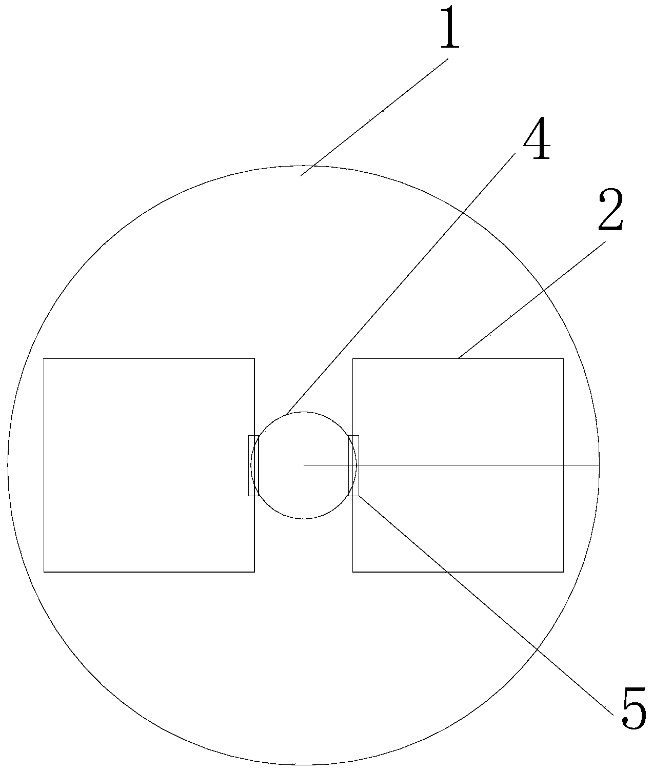
[0055] Then, use the nanoprobe to find and extract the samples on the surface of the carbon film copper mesh that cannot be observed by TEM due to the thickness is too large.

[0056] Rotate the extracted sample th...

Embodiment 2

[0060] In this embodiment, the samples that need to be re-prepared are placed on the carbon-coated copper grid and located in the damaged area of ​​the carbon-coated copper grid and cannot be observed by TEM.

[0061] The specific re-preparation method is as follows:

[0062] First, a carbon film copper grid frame with several samples placed on the surface is placed between two small silicon chips attached to the SEM / FIB sample holder, and the part of the carbon film copper grid in contact with the two small silicon chips is coated with There is silver glue to fix the carbon film copper mesh and two small silicon chips. There is a certain gap between the lower surface of the carbon film copper mesh and the SEM / FIB sample holder to ensure that subsequent nanoprobes will not be damaged due to contact with the surface of the sample holder when sampling.

[0063] Then, use the nanoprobe to find and extract the samples located in the damaged area of ​​the carbon film copper mesh t...


PUM

PropertyMeasurementUnit
thicknessaaaaaaaaaa

Abstract

The invention provides a TEM (transmission electron microscope) sample repreparation method. The method comprises: emptying the bottom of a first metal net having a surface provided with several TEM samples, and mounting it on a sample holder; seeking out a special sample needing sample repreparation from the TEM samples; transferring the special sample to a second metal net; thinning the special sample to form a finishing sample; and conducting TEM observation on the finishing sample. The method provided by the invention can screen out the special sample needing further thinning from the samples and performing further thinning, and the special sample with no need for further thinning can be directly subjected to TEM observation, thus ensuring a rapid sample preparation process, and simultaneously enhancing the success rate of sample preparation.

Description

technical field [0001] The invention relates to the field of semiconductor manufacturing, in particular to a method for re-preparing TEM samples. Background technique [0002] Currently, there are generally two methods for preparing samples for transmission electron microscopy (TEM) samples. [0003] One method is to first make a TEM sample with a thickness of about 100nm through Focused Ion Beam (FIB), and then transfer the sample through the electrostatic adsorption between the glass needle and the sample in the pickup system. to the carbon film copper grid (Grid) for subsequent TEM observations. [0004] Another method is to first make a sample with a thickness of about 500nm through FIB, then use a probe to extract the sample onto a comb-shaped copper grid, and finally perform a finishing process to make a sample that can be observed by TEM. [0005] The above two existing methods have their own advantages and disadvantages. The first method has a fast TEM sample prepa...

Claims


Application Information

Patent Timeline
Patent Type & Authority Applications(China)
IPC IPC(8): G01N1/32
Inventor 史燕萍
Owner SHANGHAI HUALI MICROELECTRONICS CORP
Why Eureka
Try Eureka