Diode and power conversion system

A diode and electrode technology, applied in the field of power conversion systems and diodes, can solve the problems of small recovery loss, disappearance of electrons and holes, etc., and achieve the effect of reducing recovery loss

Active Publication Date: 2014-03-26
HITACHI POWER SEMICON DEVICE
View PDF4 Cites 4 Cited by
  • Summary
  • Abstract
  • Description
  • Claims
  • Application Information

AI Technical Summary

Problems solved by technology

However, when the low carrier lifetime region 8 exists in the n-type negative electrode layer 3, the electrons and holes remaining in the n-type negative electrode layer on the negative electrode side cannot be efficiently eliminated during recovery.
Therefore, only through the low carrier lifetime region 8 in the n-type negative electrode layer 3, the effect of reducing the recovery loss by reducing the tail current is small

Method used


Image

  • Diode and power conversion system
  • Diode and power conversion system
  • Diode and power conversion system

Examples


no. 1 approach

[0061] [Structure of Diode]

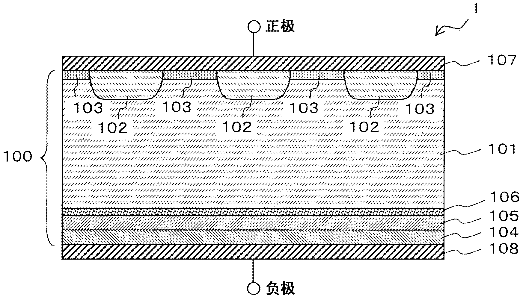
[0062] First, refer to figure 1 The structure of the diode according to the first embodiment of the present invention will be described. in addition, figure 1 is a schematic cross-sectional view of the active region of the diode 1 of the first embodiment. The description of the termination region is omitted, and a conventional termination structure such as an FLR (Field Limiting Ring) type in which p-type recesses and electrodes are arranged in a ring shape is used for the termination region.

[0063] Such as figure 1 As shown, the diode 1 of the first embodiment includes an n-drift layer 101, an anode p-layer 102, an anode p-layer 103, an anode n-layer 104, an anode buffer n-layer 105, a low lifetime region layer 106, an anode electrode 107 and an anode electrode 107. electrode 108 .

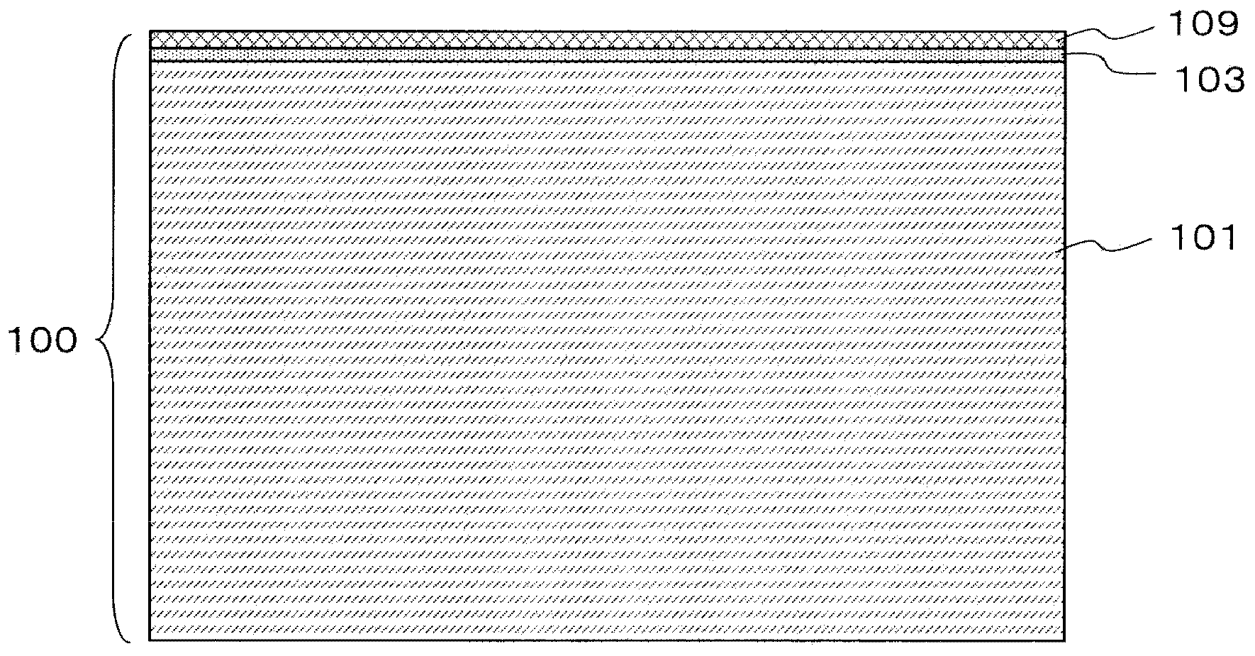
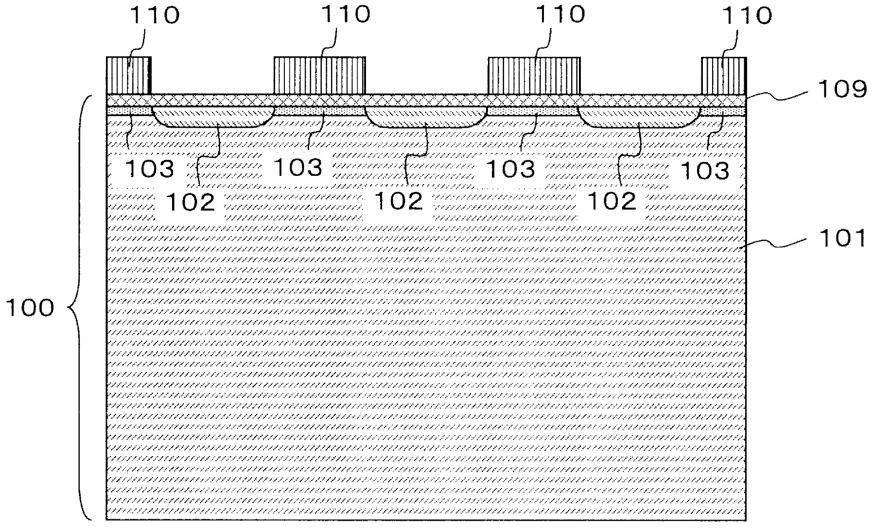
[0064] In addition, in the following description, including the intermediate stage of a manufacturing process, the whole of a semiconductor layer part is call...

no. 2 approach

[0136] Next, refer to Figure 7 Now, the structure of a diode according to a second embodiment of the present invention will be described. in addition, Figure 7 It is a schematic sectional view of the active region of the diode 1A of the second embodiment. The description of the termination region is omitted, but similar to the first embodiment, a conventional termination structure such as an FLR type in which a p-type recess and electrodes are arranged in a ring shape is used.

[0137] Such as Figure 7 As shown, the diode 1A of the second embodiment is relative to figure 1 The diode 1 of the first embodiment shown differs in that the anode p layer 102 does not have a recess structure and the anode p - layer 103, a positive electrode p-layer (second semiconductor layer) 102 is formed on the entire surface of the active region on the positive electrode side. The other structures are the same as those of the first embodiment, and description thereof will be omitted.

[0...

no. 3 approach

[0140] Next, refer to Figure 8 Now, the structure of a diode according to a third embodiment of the present invention will be described. It should be noted, Figure 8 It is a schematic sectional view of the active region of the diode 1B of the third embodiment. The description of the termination region is omitted, but similar to the first embodiment or the second embodiment, an existing termination structure such as the FLR type in which p-type recesses and electrodes are arranged in a ring shape can be used.

[0141] Such as Figure 8 As shown, the diode 1B of the third embodiment is relative to Figure 7 The diode 1A of the second embodiment shown is different in that the negative electrode buffer n layer 105 is not provided and the low lifetime region layer (fourth semiconductor layer) 106 is provided on the nth side of the negative electrode n layer (third semiconductor layer) 104. - The position where the surface on the side of the drift layer (first semiconductor la...


PUM


Abstract

The invention provides a diode that can reduce recovery loss in a simple way without accompanied voltage withstand decreases and additional procedures. The diode includes: a first semiconductor layer (101) of a first conductive type; a second semiconductor layer (102) of a second conductive type arranged adjoining to the first semiconductor layer (101); a third semiconductor layer (104) of the first conductive type which is arranged on a side, opposite to the second semiconductor layer (12), of the first semiconductor layer (101), and contains a dopant of the first conductive type at a higher concentration than the first semiconductor layer (101); a first electrode (107) ohmically connected to the second semiconductor layer (102); a second electrode (108) ohmically connected to the third semiconductor layer (104); and a fourth semiconductor layer (106) which is arranged at a position adjoining to the third semiconductor layer (104) between the first and third semiconductor layers (101, 104), contains a dopant of a type which is the same as a type of the dopant of the first conductive type contained in the third semiconductor layer (104), and has a carrier lifetime shorter than the third semiconductor layer (104).

Description

technical field [0001] The present invention relates to a diode and a power conversion system using the same. Background technique [0002] In the power conversion device, it is connected in antiparallel with IGBT (Insulated Gate Bipolar Transistor) or MOS (Metal-Oxide-Semiconductor) transistor and used as a free wheel diode. The loss of the diode is the reduction of the recovery loss. [0003] Regarding the recovery loss, the larger the tail current flowing in the diode during recovery, the larger the recovery loss becomes. Therefore, in order to reduce the recovery loss, a method of reducing the tail current has been proposed. [0004] Conventionally, as such a method, for example, a rectifier diode having a cross-sectional structure shown in FIG. 31 of Patent Document 1 has been proposed. The rectifier diode shown in FIG. 31 of Patent Document 1 has a structure in which the carrier density in the n-type negative electrode layer 281 on the negative electrode 290 side, wh...

Claims


Application Information

Patent Timeline
Patent Type & Authority Applications(China)
IPC IPC(8): H01L29/861H01L29/417
CPCH01L29/8611H01L29/66128H01L29/872H01L29/66136H01L29/66143H01L29/36
Inventor 石丸哲也森睦宏
Owner HITACHI POWER SEMICON DEVICE
Why Eureka
Try Eureka