Semiconductor device

a technology of semiconductor devices and diodes, applied in semiconductor devices, diodes, electrical devices, etc., can solve the problems deteriorating other characteristics, and large so as to reduce the recovery loss in diodes operation and suppress the effect of reducing the tolerance of switching elements

Active Publication Date: 2020-04-30
MITSUBISHI ELECTRIC CORP
View PDF0 Cites 0 Cited by
  • Summary
  • Abstract
  • Description
  • Claims
  • Application Information

AI Technical Summary

Benefits of technology

[0007]An object of the present invention is to reduce recovery loss in diode operation in a semiconductor device provided with a switching element and a diode, while suppressing reduction in tolerance of the switching element.

Problems solved by technology

The reverse conducting IGBT has several technical issues, and one of the issues is a large recovery loss in diode operation.
In the reverse conducting IGBT, there is a trade-off relation between a part of characteristics in IGBT operation and a part of characteristics in diode operation, which causes such a problem that adopting a structure for reducing recovery loss causes deterioration of other characteristics.
However, this technique requires an additional process for forming the anode region, which causes a problem of increased manufacturing cost.
Furthermore, since the anode region of the diode and a channel dope region of the IGBT are shared, there is a problem such as deterioration of a reverse bias safe operation area (RBSOA) of the IGBT.
Even with this technique, it is necessary to add a process for forming a damage layer, which causes a problem of increased manufacturing cost.
Furthermore, there is also a problem that the effect of the damage layer does not work sufficiently due to a current flow from an IGBT region where the damage layer is not formed.
As described above, the reverse conducting IGBTs of Japanese Patent Application Laid-Open No. 3-238871 (1991) and Japanese Patent Application Laid-Open No. 2008-192737 can reduce recovery loss in diode operation, but in return, problems arise such as decreased tolerance of the IGBT (such as RBSOA tolerance) and increased recovery loss due to an influence of a current from the IGBT region.

Method used


Image

  • Semiconductor device
  • Semiconductor device
  • Semiconductor device

Examples


first preferred embodiment

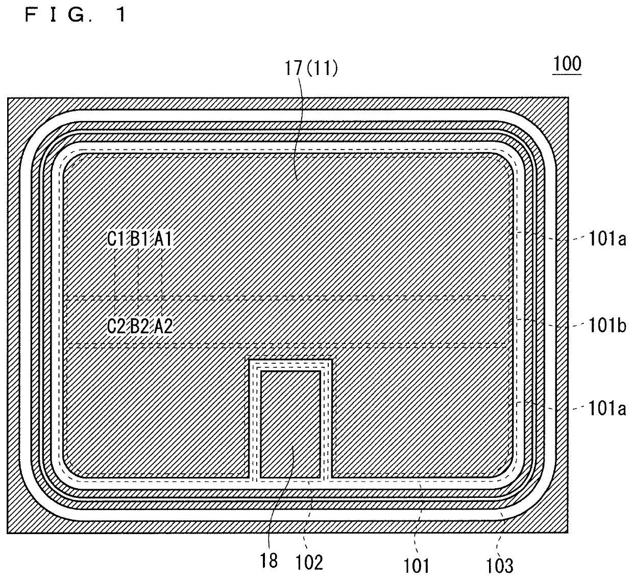
[0028]FIG. 1 is a plan view of a semiconductor chip of a reverse conducting IGBT, which is a semiconductor device 100 according to a first preferred embodiment. As shown in FIG. 1, the semiconductor device 100 includes: a main electrode region 101 formed with a main electrode 17 of the reverse conducting IGBT; a gate pad region 102 formed with a gate pad 18, which is a control electrode of the reverse conducting IGBT; and a peripheral region 103 formed with a termination structure (for example, a guard ring or the like) of the semiconductor device 100.

[0029]Under the main electrode 17, a cell of the IGBT and a cell of the diode configuring the reverse conducting IGBT are formed. That is, the main electrode region 101 is a cell region formed with the IGBT cell and the diode cell (hereinafter, the main electrode region 101 may also be referred to as a “cell region”).

[0030]As shown in FIG. 1, the main electrode region 101 is divided into an IGBT region 101a, which is a formation region...

second preferred embodiment

[0057]FIG. 6 is a plan view of a semiconductor chip of a reverse conducting IGBT, which is a semiconductor device 100 according to a second preferred embodiment. FIG. 7 is an enlarged plan view of a boundary portion between an IGBT region 101a and a diode region 101b in a cell region (main electrode region 101) of the semiconductor device 100 according to the second preferred embodiment, and shows a configuration of a surface of a semiconductor substrate. Further, FIGS. 8 to 10 are cross-sectional views of the cell region of the semiconductor device 100 according to the second preferred embodiment, in which FIG. 8 corresponds to the cross section along line D1-D2 of FIG. 7, FIG. 9 corresponds to the cross section along line E1-E2 of FIG. 7, and FIG. 10 corresponds to the cross section along line F1-F2 of FIG. 7. Note that, in FIGS. 6 to 10, elements having functions similar to those of the elements shown in FIGS. 1 to 5 are denoted by the same reference numerals, and the detailed de...

third preferred embodiment

[0063]FIG. 11 is a plan view of a semiconductor chip of a reverse conducting IGBT, which is a semiconductor device 100 according to a third preferred embodiment. FIG. 12 is an enlarged plan view of a boundary portion between an IGBT region 101a and a diode region 101b in a cell region (main electrode region 101) of the semiconductor device 100 according to the third preferred embodiment, and shows a configuration of a surface of a semiconductor substrate. Further, FIGS. 13 to 15 are cross-sectional views of the cell region of the semiconductor device 100 according to the third preferred embodiment, in which FIG. 13 corresponds to the cross section along line G1-G2 of FIG. 12, FIG. 14 corresponds to the cross section along line H1-H2 of FIG. 12, and FIG. 15 corresponds to the cross section along line I1-I2 of FIG. 12. Note that, in FIGS. 11 to 15, elements having functions similar to those of the elements shown in FIGS. 1 to 5 are denoted by the same reference numerals, and the detai...


PUM

PropertyMeasurementUnit
conductivity typeaaaaaaaaaa
conductivityaaaaaaaaaa
concentrationaaaaaaaaaa

Abstract

A semiconductor device includes an IGBT as a switching element, and a diode. The IGBT includes: a p type channel doped layer formed in a surface layer part on a front side of a semiconductor substrate; a p+ type diffusion layer and an n+ type source layer individually selectively formed in a surface layer part of the p type channel doped layer; and an emitter electrode connected to the n+ type source layer and the p+ type diffusion layer. A part of the p type channel doped layer reaches a front-side surface of the semiconductor substrate and is connected to the emitter electrode. On the front-side surface of the semiconductor substrate, the p+ type diffusion layer is interposed between the p type channel doped layer and an n+ type source layer, and the p type channel doped layer and the n+ type source layer are not adjacent to each other.

Description

BACKGROUND OF THE INVENTIONField of the Invention[0001]The present invention relates to a semiconductor device, and particularly to a semiconductor device including a switching element and a diode, such as a reverse conducting IGBT.Description of the Background Art[0002]In general, semiconductor devices (power devices) for power control have various requirements such as breakdown-voltage holding capability and guarantee of a safe operation area (current / voltage area for an element not to be destroyed in operation), and one of the requirements is loss reduction. The loss reduction of power devices has an effect of reducing size and weight of the device, and an effect of accordingly leading to consideration of the global environment by reduction of energy consumption. Furthermore, there is a demand for realizing these characteristics at the lowest possible cost. As one means to respond to such a demand, there has been proposed a reverse-conducting insulated gate bipolar transistor (RC...

Claims


Application Information

Patent Timeline
Patent Type & Authority Applications(United States)
IPC IPC(8): H01L27/06H01L29/739H01L29/861
CPCH01L27/0647H01L29/861H01L29/7393H01L29/7396H01L29/0603H01L29/0684H01L29/8613H01L29/407H01L29/32H01L29/0696H01L29/7397H01L29/402H01L29/66348H01L27/0727H01L29/0834H01L29/1095
Inventor TAKAHASHI, TETSUOKANEDA, MITSURU
Owner MITSUBISHI ELECTRIC CORP
Why Eureka
Try Eureka