Reverse conduction semiconductor device and method for manufacturing reverse conduction semiconductor device

A technology of reverse conduction and semiconductor, which is applied in semiconductor/solid-state device manufacturing, semiconductor devices, electric solid-state devices, etc., can solve the problems of increased manufacturing cost, concentration difference, and complicated impurity addition process, and achieve high latch-up tolerance, Avoid manufacturing costs, avoid greatly increased effects

Pending Publication Date: 2022-04-22
MITSUBISHI ELECTRIC CORP
View PDF1 Cites 1 Cited by
  • Summary
  • Abstract
  • Description
  • Claims
  • Application Information

AI Technical Summary

Problems solved by technology

On the other hand, in order to provide such a difference in concentration, generally, it is necessary to greatly complicate the impurity addition process, and as a result, the manufacturing cost increases significantly.

Method used


Image

  • Reverse conduction semiconductor device and method for manufacturing reverse conduction semiconductor device
  • Reverse conduction semiconductor device and method for manufacturing reverse conduction semiconductor device
  • Reverse conduction semiconductor device and method for manufacturing reverse conduction semiconductor device

Examples


Embodiment approach 2

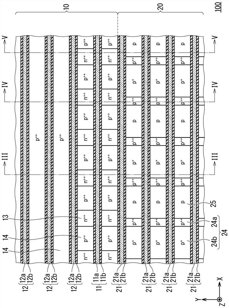
[0126] Figure 17 so with figure 2 The same field of view schematically shows a partial plan view of the structure of the RC-IGBT 102 (reverse conduction type semiconductor device) viewed along the upper surface (first main surface) of the semiconductor substrate 50 according to the second embodiment. In Embodiment 2, the same as Embodiment 1 ( figure 2 ) different, p + The anode contact layer 24b is p ++ The anode contact layer 24a surrounds the configuration at p ++ The inner side of the anode contact layer 24a. In addition, since the configuration other than that is substantially the same as that of the above-mentioned first embodiment, the same or corresponding elements are given the same reference numerals, and the description thereof will not be repeated.

[0127] In common with Embodiments 1 and 2, in p + The anode contact layer 24b is provided with a p-type by further counter-doping an acceptor to a region where a donor is added. Therefore, at the upper surfac...

Embodiment approach 5

[0136] Figure 20 so with Figure 17 The same field of view schematically shows a partial plan view of the structure of the RC-IGBT 105 (reverse conduction type semiconductor device) viewed along the upper surface (first main surface) of the semiconductor substrate 50 according to the fifth embodiment. In Embodiment 5, the same as Embodiment 2 ( Figure 17 ) different, p ++ Anode contact layer 24a is p + The anode contact layer 24b surrounds the configuration at p + The inner side of the anode contact layer 24b. In other words, transposing p ++ Anode contact layer 24a and p + Configuration of the anode contact layer 24b. In addition, since the configuration other than that is substantially the same as that of the above-mentioned second embodiment, the same or corresponding elements are given the same reference numerals, and the description thereof will not be repeated.

[0137] According to the present embodiment, the density of holes injected into the p-type anode lay...

Embodiment approach 6

[0139] Figure 21 so with figure 2 The same field of view schematically shows a partial plan view of the structure of the RC-IGBT 106 (reverse conduction type semiconductor device) viewed along the upper surface (first main surface) of the semiconductor substrate 50 according to the sixth embodiment. In this embodiment, with Embodiment 5 ( Figure 20 ) is different from p + Anode contact layer 24b surrounded by p ++ The anode contact layer 24a is scattered and arranged in a zigzag shape. In addition, since the configuration other than that is substantially the same as that of the above-mentioned fifth embodiment, the same reference numerals are attached to the same or corresponding elements, and the description thereof will not be repeated.

[0140] According to this embodiment 6 ( Figure 21 ), and Embodiment 5 ( Figure 20 ), the hole current density at the diode region 20 becomes more equal. Thereby, the heat dissipation of the diode region 20 can be improved.


PUM

PropertyMeasurementUnit
electrical resistivityaaaaaaaaaa

Abstract

The invention relates to a reverse conducting semiconductor device and a manufacturing method of the reverse conducting semiconductor device. Provided is a reverse-conducting semiconductor device having high latch-up tolerance and low recovery loss while avoiding a significant increase in manufacturing cost. The semiconductor substrate (50) has a first main surface (F1) and a second main surface (F2). The base contact layer (14) is disposed between the base layer (15) and the first main surface (F1) and constitutes a part of the first main surface (F1). The anode contact region (24) is disposed between the anode layer (25) and the first main surface (F1), constitutes a part of the first main surface (F1), and has a second conductivity-type impurity concentration peak higher than that of the anode layer (25). The anode contact region (24) includes a first anode contact layer (24b) having a lower net concentration than the base contact layer (14) and a higher first conductivity type impurity concentration than the base contact layer (14).

Description

technical field [0001] The present invention relates to a reverse conduction type semiconductor device and a method for manufacturing the reverse conduction type semiconductor device. Background technique [0002] For power modules that perform variable-speed control of three-phase motors in fields such as general-purpose inverters and AC servos, from the viewpoint of energy saving, insulated gate bipolar transistors (IGBT: Insulated Gate Bipolar Transistor) and freewheeling diodes are used. In this case, compared with using both a semiconductor device as an IGBT and a semiconductor device as a freewheel diode (diode for reverse conduction), by using a reverse conduction type semiconductor device having an IGBT region and a diode region, That is, the reverse conducting IGBT (RC-IGBT: Reverse Conducting IGBT), which can reduce the area occupied by the IGBT and the diode in the power module. Therefore, the power module can be downsized. [0003] For example, International Pu...

Claims


Application Information

Patent Timeline
Patent Type & Authority Applications(China)
IPC IPC(8): H01L29/06H01L29/08H01L29/739H01L29/861H01L27/07H01L21/329H01L21/331H01L21/822
CPCH01L27/0727H01L21/822H01L29/7398H01L29/7397H01L29/8613H01L29/66136H01L29/66348H01L29/0684H01L29/0804H01L29/407H01L29/0692H01L29/0619H01L29/0696H01L29/861
Inventor 西康一曾根田真也中谷贵洋
Owner MITSUBISHI ELECTRIC CORP
Why Eureka
Try Eureka