Converter and power conversion device using same

a technology of converter and power conversion device, which is applied in the direction of efficient power electronics conversion, emergency power supply arrangement, climate sustainability, etc., can solve the problems of reducing the cost of the converter, reduce the size and cost of the device, reduce the loss of switching and recovery, and reduce the cost

Active Publication Date: 2020-04-21
TOSHIBA MITSUBISHI-ELECTRIC IND SYST CORP
View PDF15 Cites 0 Cited by
  • Summary
  • Abstract
  • Description
  • Claims
  • Application Information

AI Technical Summary

Benefits of technology

[0007]The converter according to the present invention includes three transistors and six diodes. This converter accordingly has fewer semiconductor elements than a conventional converter, thus reducing the size and cost of the device. Further, the first and second diodes that perform the reverse recovery operation and the third transistor that switches a large current are made of wide bandgap semiconductors, thus reducing a switching loss and a recovery loss. The third to sixth diodes that do not perform the reverse recovery operation and the first and second transistors that switch a small current are made of semiconductors other than wide bandgap semiconductors, leading to a reduced cost.

Problems solved by technology

Besides, the other four diodes that do not perform the reverse recovery operation are made of semiconductors other than wide bandgap semiconductors, leading to a reduced cost of the converter.

Method used


Image

  • Converter and power conversion device using same
  • Converter and power conversion device using same
  • Converter and power conversion device using same

Examples


embodiment 1

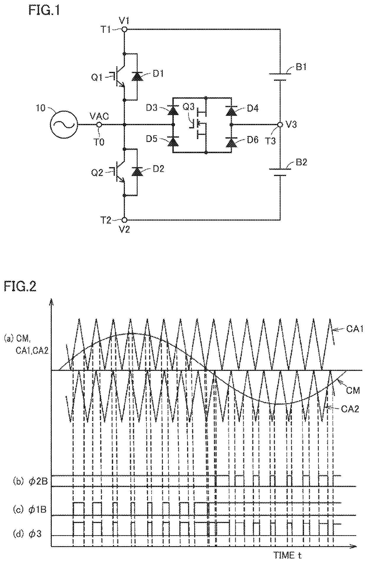
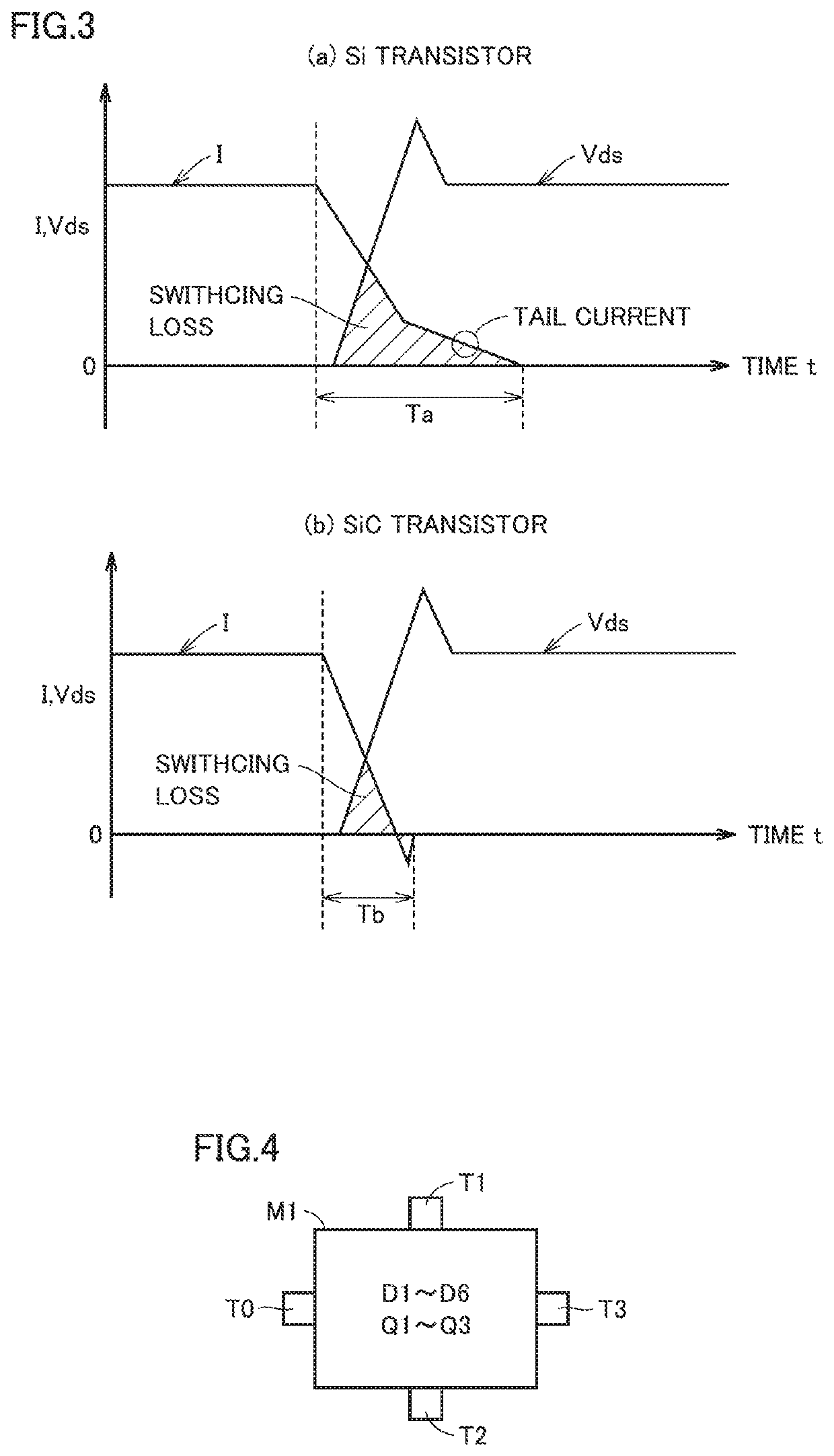
[0023]FIG. 1 is a circuit diagram showing a configuration of a converter according to Embodiment 1 of the present invention. With reference to FIG. 1, this converter includes an input terminal T0, output terminals T1 to T3 (first to third output terminals), diodes D1 to D6 (first to sixth diodes), and transistors Q1 to Q3 (first to third transistors).

[0024]Input terminal T0 receives an AC voltage VAC of a commercial frequency from, for example, a commercial AC power supply 10. Output terminals T1 and T3 are connected respectively with the positive electrode and negative electrode of a battery B1. Output terminals T3 and T2 are connected respectively with the positive electrode and negative electrode of a battery B2. Each of batteries B1 and B2 stores DC power. Batteries B1 and B2 are charged with DC voltages having the same value.

[0025]When the voltages at output terminals T1, T2, and T3 are respectively DC voltages V1, V2, and V3, V1>V3>V2, and V3=(V1+V2) / 2. This converter converts...

embodiment 2

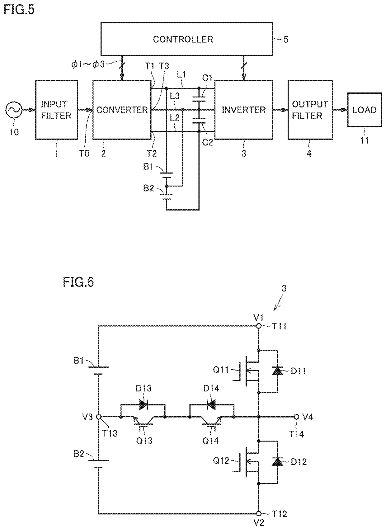
[0077]FIG. 6 is a circuit block diagram showing a configuration of inverter 3 of an uninterruptible power system according to Embodiment 2 of the present invention. The general arrangement of the uninterruptible power system is as shown in FIG. 5. Converter 2 of the uninterruptible power system is the converter shown in FIG. 1. With reference to FIG. 6, inverter 3 includes input terminals T11 to T13 (first to third output terminals), an output terminal T14 (fourth output terminal), transistors Q11 to Q14 (fourth to seventh transistors), and diodes D11 to D14 (seventh to tenth diodes).

[0078]Input terminals T11 to T13 are connected respectively to DC positive bus L1, DC negative bus L2, and DC neutral point bus L3 of FIG. 5. Input terminals T11 and T13 are connected respectively with the positive electrode and negative electrode of battery B1. Input terminals T13 and T12 are connected respectively with the positive electrode and negative electrode of battery B2. Each of batteries B1 a...

embodiment 3

[0112]FIG. 11 is a circuit diagram showing a configuration of an inverter of an uninterruptible power system according to Embodiment 3 of the present invention, which is compared with FIG. 6. With reference to FIG. 11, this inverter differs from inverter 3 of FIG. 6 in that the parallel connection structure of transistor Q13 and diode D13 and the parallel connection structure of transistor Q14 and diode D14 are replaced. Transistors Q13 and Q14 have emitters connected to each other and collectors connected respectively to input terminal T13 and output terminal T14. Transistors Q11 to Q14 are controlled respectively by PWM signals φ11 to φ14. When DC voltages V1 and V3 are alternately output to output terminal T14, transistor Q14 is turned on and transistors Q11 and Q13 are alternately turned on. When DC voltages V2 and V3 are alternately output to output terminal T14, transistor Q13 is turned on and transistors Q12 and Q14 are alternately turned on.

[0113]Since the other configuratio...


PUM

PropertyMeasurementUnit
DC voltagesaaaaaaaaaa
rated currentaaaaaaaaaa

Abstract

A converter includes a first diode having an anode and a cathode connected respectively to an input terminal and a first output terminal, a second diode having an anode and a cathode connected respectively to a second output terminal and the input terminal, a first transistor connected between the first output terminal and the input terminal, a second transistor connected between the input terminal and the second output terminal, and a bidirectional switch connected between the input terminal and a third output terminal and including third to sixth diodes and a third transistor. Each of the first diode, the second diode, and the third transistor is made of a wide bandgap semiconductor. Each of the first and second transistors and the third to sixth diodes is made of a semiconductor other than the wide bandgap semiconductor.

Description

TECHNICAL FIELD[0001]The present invention relates to a converter and a power conversion apparatus including the same, and particularly, to a converter that converts an AC voltage into first to third DC voltages and a power conversion apparatus including the converter.BACKGROUND ART[0002]Japanese Patent Laying-Open No. 2011-78296 (PTD 1) discloses a converter that includes four transistors and six diodes and converts an AC voltage into a high voltage, a low voltage, and an intermediate voltage. Two diodes that perform a reverse recovery operation among the six diodes are made of wide bandgap semiconductors, leading to a reduced recovery loss of the converter. Besides, the other four diodes that do not perform the reverse recovery operation are made of semiconductors other than wide bandgap semiconductors, leading to a reduced cost of the converter.CITATION LISTPatent Document[0003]PTD 1: Japanese Patent Laying-Open No. 2011-78296SUMMARY OF INVENTIONTechnical Problem[0004]A conventio...

Claims


Application Information

Patent Timeline
Patent Type & Authority Patents(United States)
IPC IPC(8): H02M7/12H02M7/483H02M1/32H02M1/00
CPCH02M7/12H02M1/32H02M7/483H02M2001/0054H02M2001/0006H02M5/4585H02M7/217H02M7/487H02M7/5395H02M7/797H02J9/062Y02B70/10H02M1/0051H02M1/0054H02M1/0006
Inventor OHNISHI, KEISUKEABE, SHOICHISANADA, KAZUNORI
Owner TOSHIBA MITSUBISHI-ELECTRIC IND SYST CORP
Why Eureka
Try Eureka