Power semiconductor device

a technology of semiconductor devices and power semiconductors, applied in semiconductor devices, diodes, electrical devices, etc., can solve the problems of low efficiency of the whole system, disadvantageous magnitude of reverse current at the turn-off, and increase in recovery loss, so as to reduce recovery loss

Active Publication Date: 2007-07-17
MITSUBISHI ELECTRIC CORP
View PDF4 Cites 1 Cited by
  • Summary
  • Abstract
  • Description
  • Claims
  • Application Information

AI Technical Summary

Benefits of technology

[0011]It is an object of the present invention to provide a power semiconductor device which makes the impurity diffusion length of an anode electrode region shallower in order to ensure reduction in recovery loss.
[0013]The power semiconductor device of the present invention can eliminate necessity for the mesa portion to perform the function of relieving the electric field (or can reduce the degree of dependency on the mesa portion for field relieving function) in applying a reverse voltage. Accordingly, it is possible to set the impurity diffusion length of the second main electrode region smaller than the height of the vertical portion. Thus, since the impurity diffusion length of the second main electrode region can be made smaller (shallower), it is possible to reduce the reverse current at the turn-off. Therefore, by equipping a system with the power semiconductor device of the first aspect, it is possible to increase the efficiency of the whole system.

Problems solved by technology

Thus, as the impurity diffusion length (height) of the anode electrode region becomes longer (higher), the magnitude of a reverse current at the turn-off disadvantageously increases (in other words, a recovery loss increases).
If a predetermined system carries the thyristor with large recovery loss, the efficiency of the whole system becomes low.

Method used


Image

  • Power semiconductor device
  • Power semiconductor device
  • Power semiconductor device

Examples


Embodiment Construction

[0025]Hereinafter, the present invention will be discussed specifically, referring to figures showing preferred embodiments.

The First Preferred Embodiment

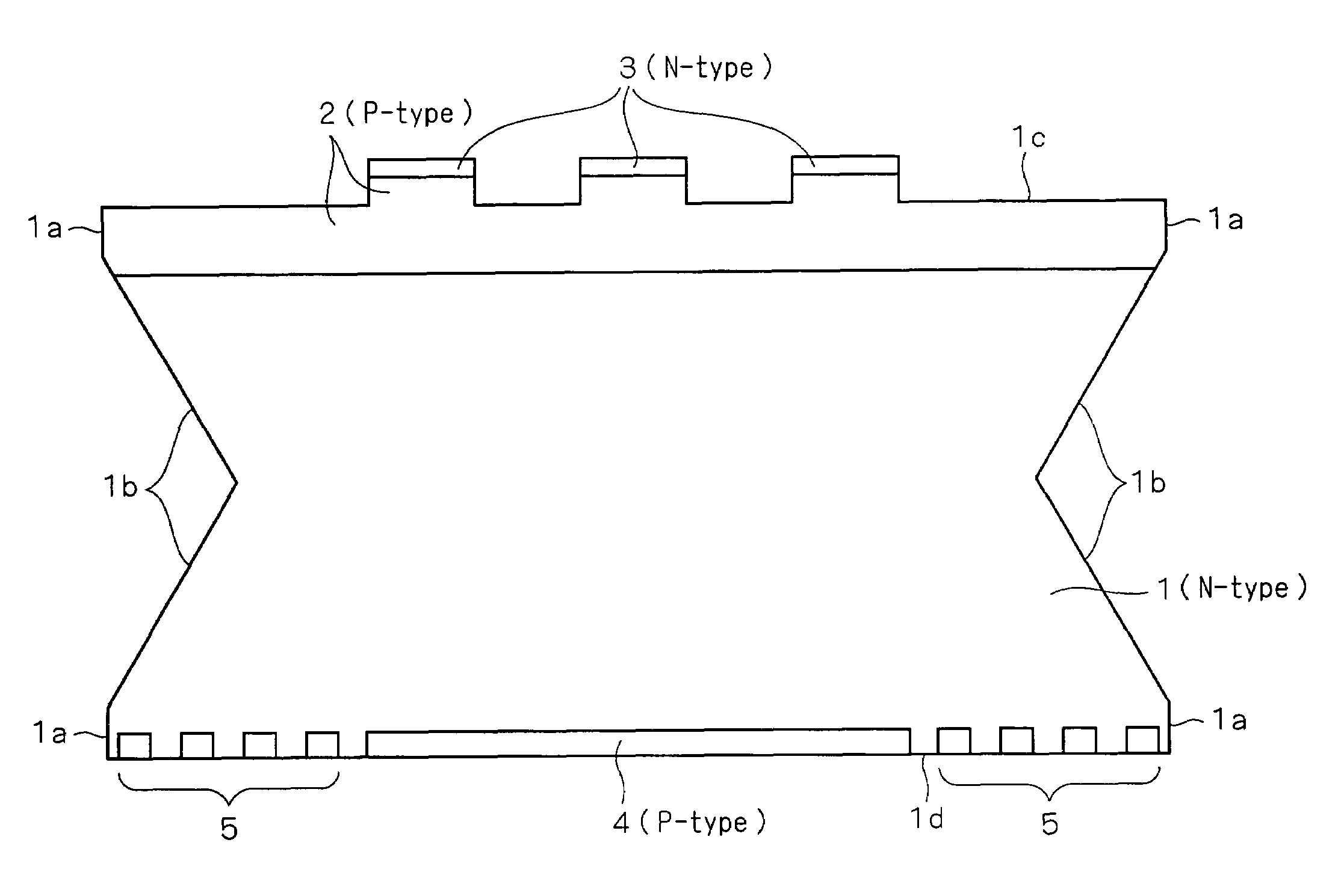
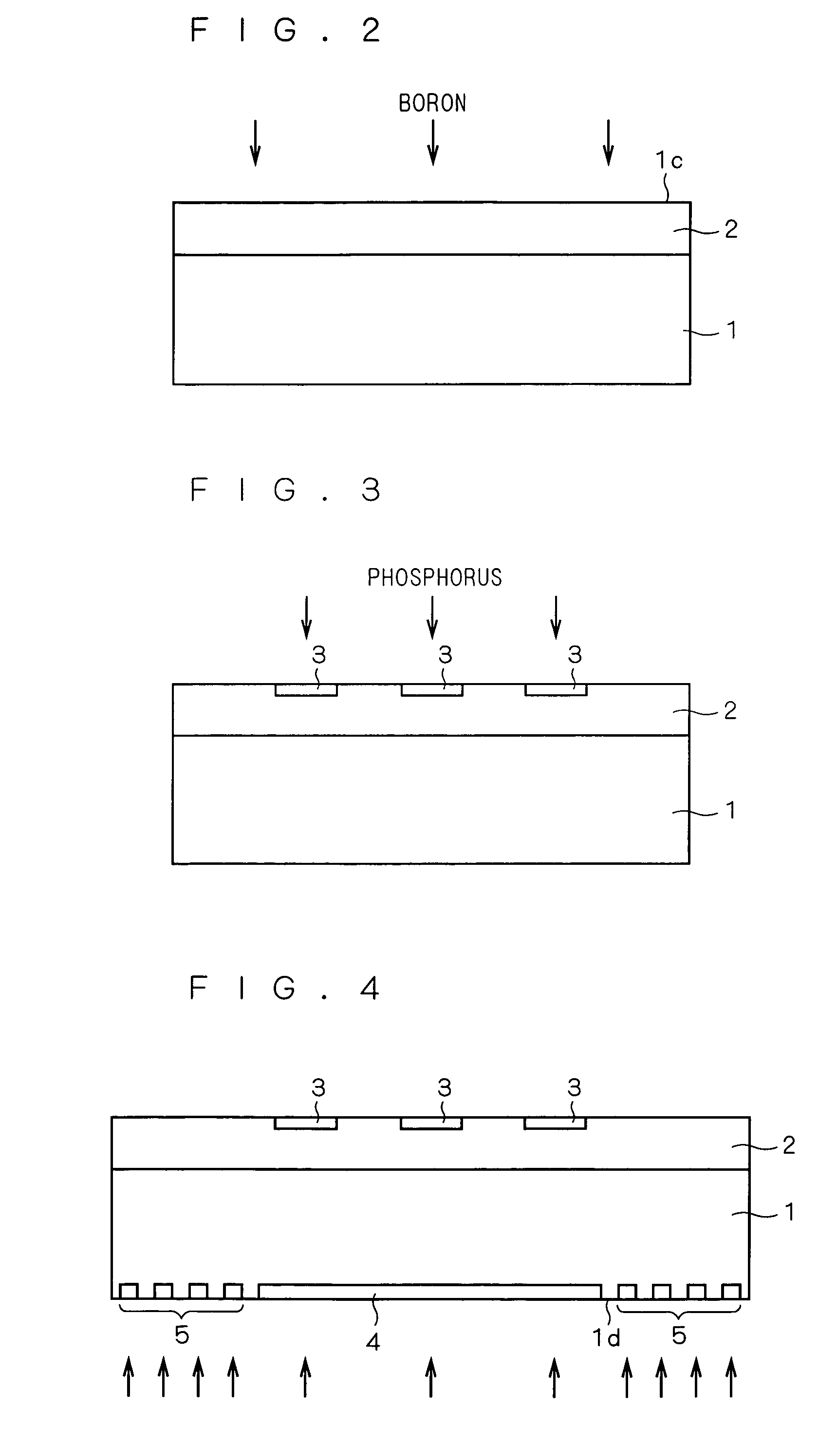
[0026]FIG. 1 is a cross section showing a structure of a power semiconductor device in accordance with the first preferred embodiment of the present invention. Discussion will be made below on a thyristor (especially, an NPNP-type thyristor), however, the present invention can be applied to a power transistor such as an IGBT (Insulated Gate Bipolar Transistor) or the like.

[0027]FIG. 1 shows an N-type (first conductivity type) semiconductor substrate 1. A side surface portion of the semiconductor substrate 1 has the following shape in a cross section. Specifically, the side surface portion of the semiconductor substrate 1 has a vertical portion 1a formed substantially vertical to a main surface and a mesa portion 1b connected to the vertical portion 1a.

[0028]In other words, as shown in FIG. 1, the side surface portion has the verti...


PUM


Abstract

A power semiconductor device comprises a semiconductor substrate, a gate electrode region (control electrode region), a cathode electrode region (first main electrode region), an anode electrode region (second main electrode region) and a guard ring. The semiconductor substrate has a side surface portion having a vertical portion formed substantially vertical to a main surface and a mesa portion connected to the vertical portion in a cross section. The gate electrode region is formed in a first main surface of the semiconductor substrate. The cathode electrode region is formed in part of a surface of the gate electrode region. The anode electrode region is formed in a second main surface of the semiconductor substrate. The guard ring is formed in the second main surface of the semiconductor substrate and annularly surrounds the anode electrode region. With this constitution provided is a power semiconductor device which makes the impurity diffusion length of the anode electrode region shallower in order to ensure reduction in recovery loss.

Description

BACKGROUND OF THE INVENTION[0001]1. Field of the Invention[0002]The present invention relates to a power semiconductor device and can be applied to, e.g., a thyristor, an IGBT or the like.[0003]2. Description of the Background Art[0004]In a general-type structure of a reverse blocking thyristor, conventionally, in a lower surface of a semiconductor substrate of a first conductivity type, an anode electrode region of a second conductivity type is formed.[0005]Both side surface portions of the semiconductor substrate have a mesa structure. A lower side surface end of the semiconductor substrate, however, has a portion which is substantially vertical to a lower surface (hereinafter, referred to as “vertical portion”) in order to prevent a crack in a manufacturing process or the like. In other words, in a predetermined range from the lower surface of the semiconductor substrate, the side surface portion of the semiconductor substrate is the vertical portion and the vertical portion is c...

Claims


Application Information

Patent Timeline
Patent Type & Authority Patents(United States)
IPC IPC(8): H01L29/74H01L31/111
CPCH01L29/0661H01L29/0834H01L29/74H01L29/0619H01L29/87
Inventor OOTA, KENJIYAMAGUCHI, YOSHIHIROYAMAGUCHI, HIROSHI
Owner MITSUBISHI ELECTRIC CORP
Why Eureka
Try Eureka