Organic electroluminescence display, optical thin film stacking body of organic electroluminescence display and preparing method of optical thin film stacking body

An electroluminescent display and optical thin film technology, which is applied in the manufacture of organic semiconductor devices, electrical solid state devices, semiconductor/solid state devices, etc., can solve the problems of cumbersome process, difficult curling of flexible organic electroluminescent display devices, and high cost. To achieve the effect of solving the cumbersome process, avoiding the difficulty of curling, and solving the cost increase

Inactive Publication Date: 2014-03-26
BOE TECH GRP CO LTD
View PDF5 Cites 17 Cited by
  • Summary
  • Abstract
  • Description
  • Claims
  • Application Information

AI Technical Summary

Problems solved by technology

[0006] Embodiments of the present invention provide an optical thin film laminate for an organic electroluminescent display device, a preparation method thereof, an organic electroluminescent display device and a display device, so as to solve the two-dimensional problem of the existing organic electroluminescent display device. The problems of cumbersome process, high cost and difficult curling of flexible organic electroluminescent display devices caused by sub-film

Method used


Image

  • Organic electroluminescence display, optical thin film stacking body of organic electroluminescence display and preparing method of optical thin film stacking body
  • Organic electroluminescence display, optical thin film stacking body of organic electroluminescence display and preparing method of optical thin film stacking body
  • Organic electroluminescence display, optical thin film stacking body of organic electroluminescence display and preparing method of optical thin film stacking body

Examples


Embodiment Construction

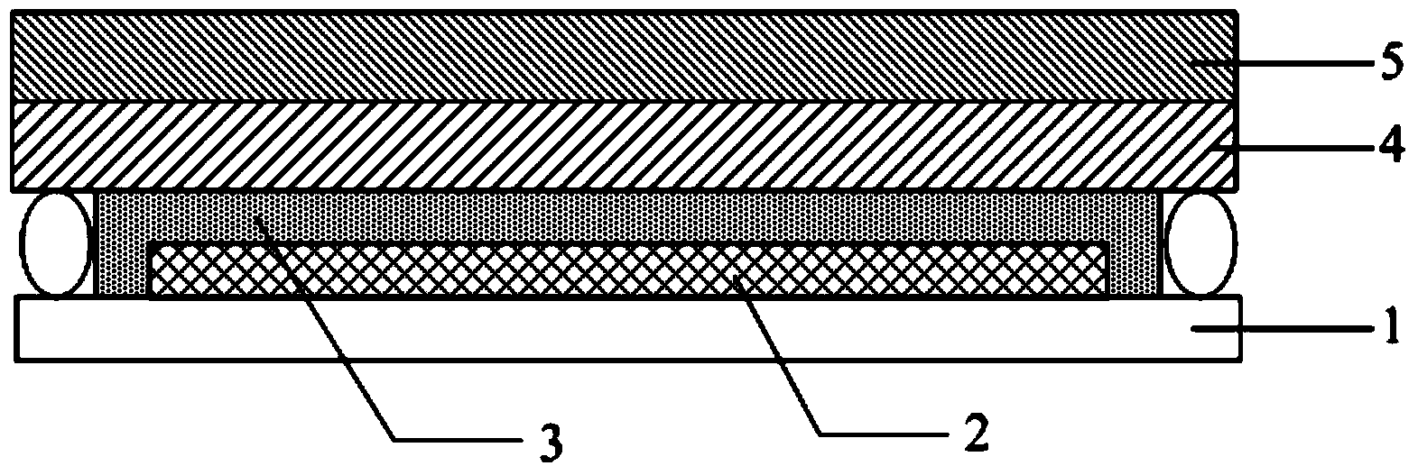
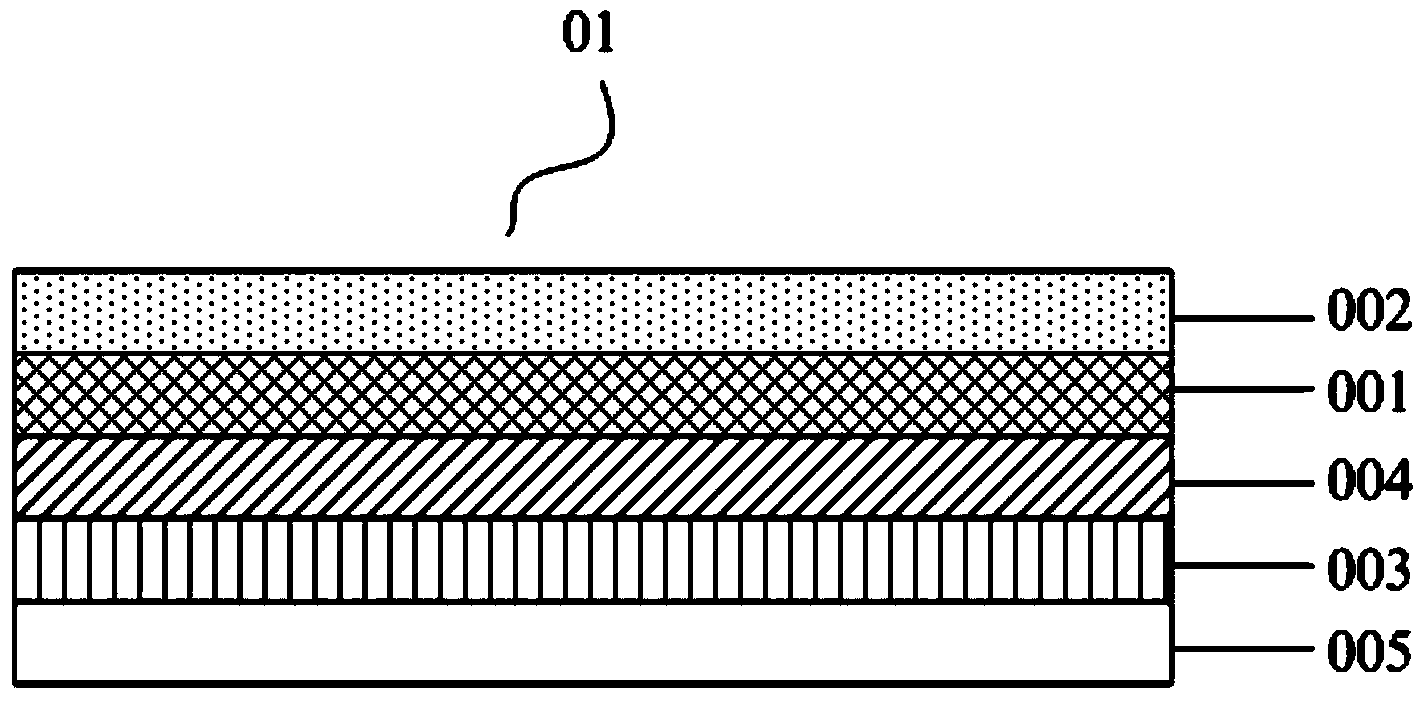
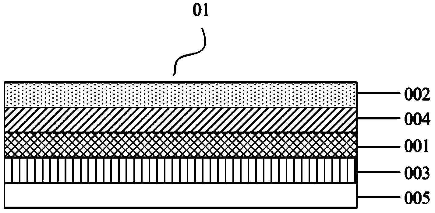
[0040] The specific embodiments of the optical thin film laminate for organic electroluminescent display devices, its preparation method, organic electroluminescent display device and display device provided by the embodiments of the present invention will be described in detail below with reference to the accompanying drawings.

[0041] Wherein, the film thickness of each layer in the drawings does not reflect the real ratio of the optical film laminate and the organic electroluminescent display device, and the purpose is only to illustrate the content of the present invention.

[0042] An optical film laminate 01 for an organic electroluminescent display device provided by an embodiment of the present invention, such as Figure 2a to Figure 2c As shown, it includes: a circular polarizer film layer 001, a protective film layer 002 located on the light incident side of the circular polarizer film layer 001, an adhesive layer 003 located on the light exit side of the circular po...


PUM


Abstract

The invention discloses an organic electroluminescence display, an optical thin film stacking body of the organic electroluminescence display and a preparing method of the optical thin film stacking body. The optical thin film stacking body comprises a circular polaroid film layer, a protection film layer located on the incident side of the circular polaroid film layer, a binding layer located on the light-emitting side of the circular polaroid film layer and a water blocking oxygen film layer. The water blocking oxygen film layer is located between the light-emitting side of the circular polaroid film layer and the binding layer, and/or located between the incident side of the circular polaroid film layer and the protection film layer. Due to the fact that the optical thin film stacking body comprises the circular polaroid film layer and the water blocking oxygen film layer, the optical thin film stacking body has the anti-reflection function and the good water blocking oxygen property. When the optical thin film stacking body with the double functions is applied to the OLED, the problems, caused by secondary pasting, of the complex technological process, high cost and soft OLED crimping difficulty and the like are solved, and meanwhile the OLED can have the advantages of being lighter, thinner, better in displaying effect and the like.

Description

technical field [0001] The invention relates to the field of display technology, in particular to an optical film laminate used for an organic electroluminescence display device, a preparation method thereof, an organic electroluminescence display device and a display device. Background technique [0002] At present, compared with traditional liquid crystal display devices (Liquid Crystal Display, LCD), organic electroluminescent display devices (Organic Electroluminescent Display, OLED) have the characteristics of fast response, wide color gamut, ultra-thin, and flexibility. Has gradually become the mainstream of the display field. [0003] The structure of the OLED display device mainly includes: a base substrate, an organic electroluminescent pixel array fabricated on the substrate substrate; wherein, each organic electroluminescent pixel array includes an anode and a cathode arranged oppositely, and between the luminous layers. The light emission of the OLED display de...

Claims


Application Information

Patent Timeline
Patent Type & Authority Applications(China)
IPC IPC(8): H01L51/52H01L27/32H01L51/56
CPCH10K59/10H10K50/8445H10K50/844H10K50/86H10K71/00Y02E10/549G02B5/3033G02B1/14Y02P70/50H10K77/111H10K50/841H10K2102/311H10K50/8426H10K59/12H10K85/40H10K85/141H10K2102/00G02B5/3041
Inventor 高雪刘飞曾庆慧王俊然廖金龙
Owner BOE TECH GRP CO LTD
Why Eureka
Try Eureka