High-speed serial-parallel conversion circuit based on FPGA
A conversion circuit, high-speed technology, applied in parallel/serial conversion, code conversion, electrical components, etc., can solve the problems of complex realization, fixed structure, limited application scope, etc., and achieve the effect of cost reduction
- Summary
- Abstract
- Description
- Claims
- Application Information
AI Technical Summary
Problems solved by technology
Method used
Image

Examples
Embodiment Construction
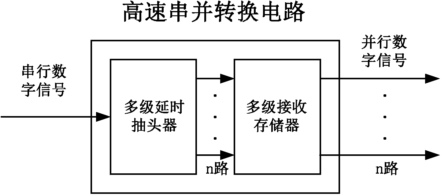
[0017] The FPGA-based high-speed serial-to-parallel conversion circuit of the present invention can collect and output multiple bits in parallel after passing the high-speed serial digital signal through the FPGA-based multi-stage delay tap device and multi-stage receiving memory under the low-speed clock. Digital signal.
[0018] The present invention is based on the high-speed serial-to-parallel conversion circuit of FPGA, and its realization circuit is made up of multi-stage delay tap device and multi-stage receiving memory two parts, and realization method is as follows:
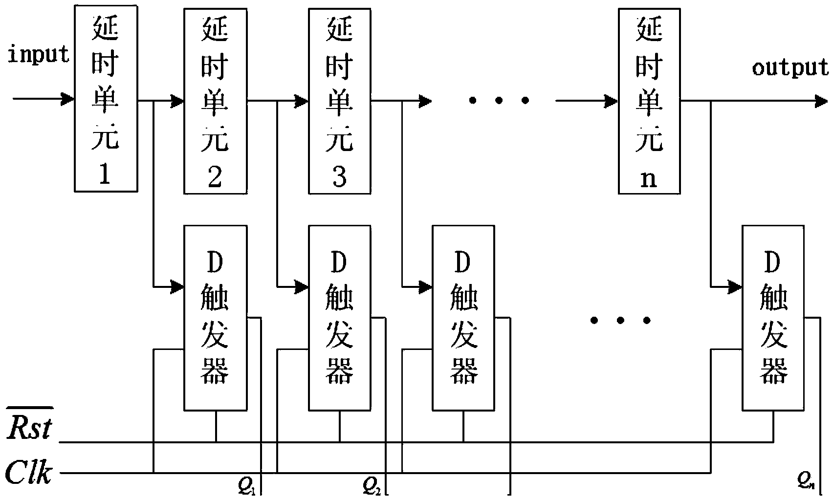
[0019] 1. The high-speed digital signal enters the multi-level delay tap to output the multi-level delayed signal;
[0020] Second, the delay signals at all levels correspond to the D flip-flops input to the multi-level receiving memory. When the next clock arrives, the current input D flip-flop signal is stored and output, thereby realizing the serial to parallel conversion of signals within a single cl...
PUM
 Abstract
Description
Claims
Application Information
 - R&D
- Intellectual Property
- Life Sciences
- Materials
- Tech Scout
- Unparalleled Data Quality
- Higher Quality Content
- 60% Fewer Hallucinations
Browse by: Latest US Patents, China's latest patents, Technical Efficacy Thesaurus, Application Domain, Technology Topic, Popular Technical Reports.
© 2025 PatSnap. All rights reserved.Legal|Privacy policy|Modern Slavery Act Transparency Statement|Sitemap|About US| Contact US: help@patsnap.com