Isolation pad detecting device and method
A detection device and detection method technology, applied in nonlinear optics, instruments, optics, etc., can solve the problems of inaccurate measurement, abnormal liquid crystal cell thickness, and relatively high requirements for device vibration, and achieve the effect of simple detection equipment
- Summary
- Abstract
- Description
- Claims
- Application Information
AI Technical Summary
Problems solved by technology
Method used
Image

Examples
Embodiment 1
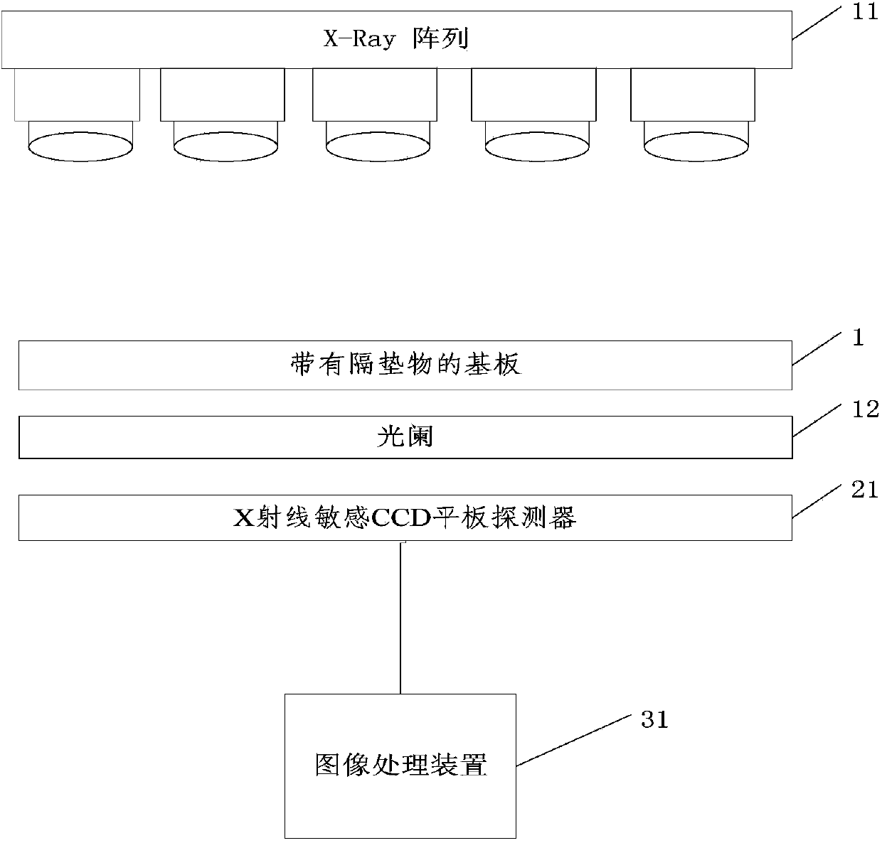
[0037] This embodiment proposes a spacer detection device, including: an X-ray imaging unit and an image processing unit, wherein the X-ray imaging unit includes an X-ray source and an X-ray sensitive lens;
[0038] X-ray source for generating X-rays transmitted through the substrate with the spacer;
[0039] X-ray sensitive lens, which receives X-rays passing through the substrate and forms a grayscale image;
[0040] The image processing unit measures the height of the spacer by using the grayscale image.
[0041] In this embodiment, the X-ray source is an X-ray array source, and the X-ray sensitive lens is an X-ray sensitive CCD flat panel detector. Specifically, such as figure 1 As shown, an X-ray array source 11 controlled by an X-ray controller (not shown in the figure) emits X-rays to the substrate 1 with spacers. X-ray sensitive CCD Flat Panel Detector (Flat Panel Detector, FPD) 21 is a kind of FPD that obtains images indirectly, mainly consists of a scintillator or...
Embodiment 2
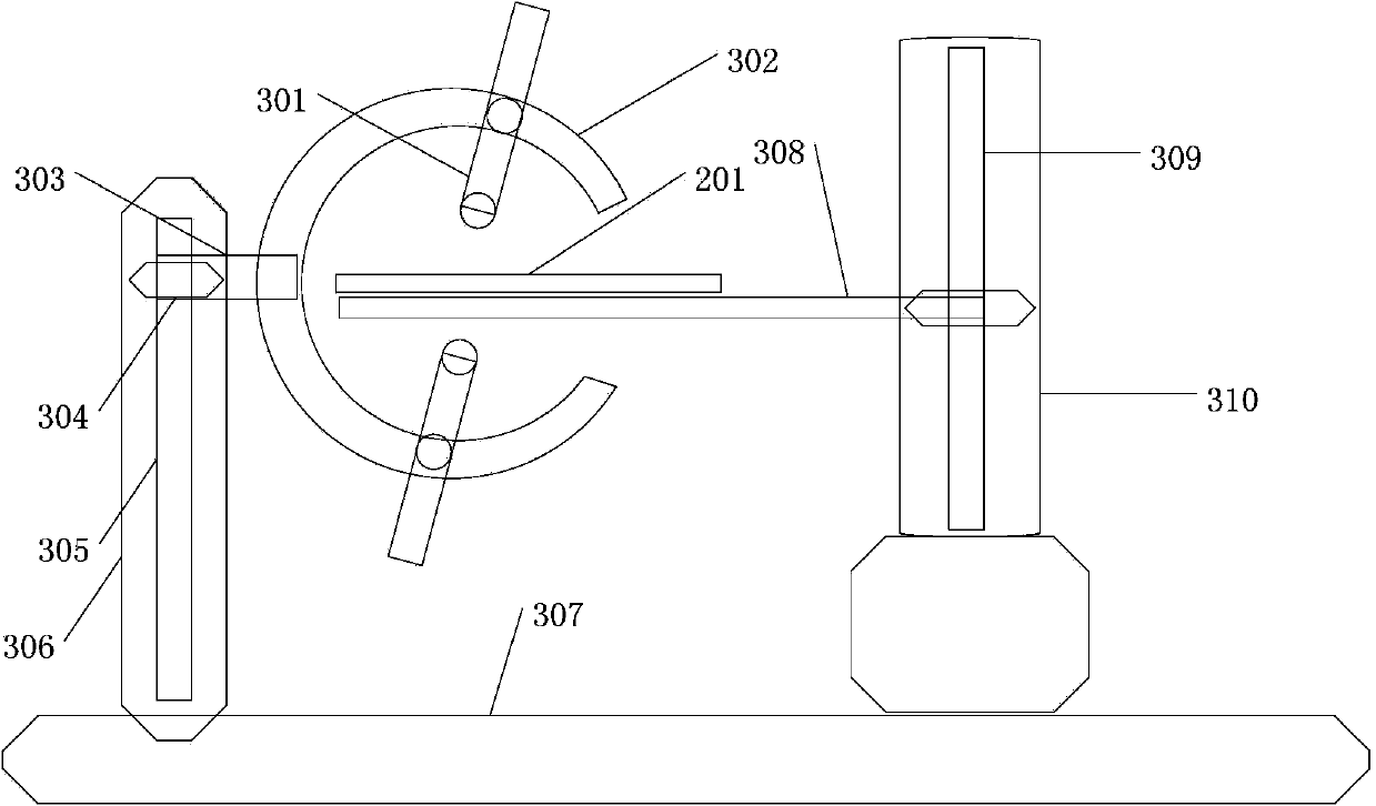
[0059] The difference between the spacer detection device of this embodiment and the first embodiment lies in the X-ray imaging unit, that is, the mechanical structure of the device and the optical structure of the X-ray imaging unit. There are two X-ray imaging units in this embodiment, which are opposite to each other with respect to the substrate. The X-ray sensitive lens of any one of the X-ray imaging units receives the X-rays transmitted through the substrate by the X-ray source of the other X-ray imaging unit, forming gray degree image. And the two X-ray imaging units can move on the arc track, so that the angle at which the X-rays enter the substrate changes. The specific structure of the spacer detection device of this embodiment is as follows: figure 2 shown. A pair of X-ray imaging units 301 are installed on the circular arc track 302 and can move on the circular arc track 302, but they are always relatively arranged in a straight line to facilitate imaging. The...
Embodiment 3
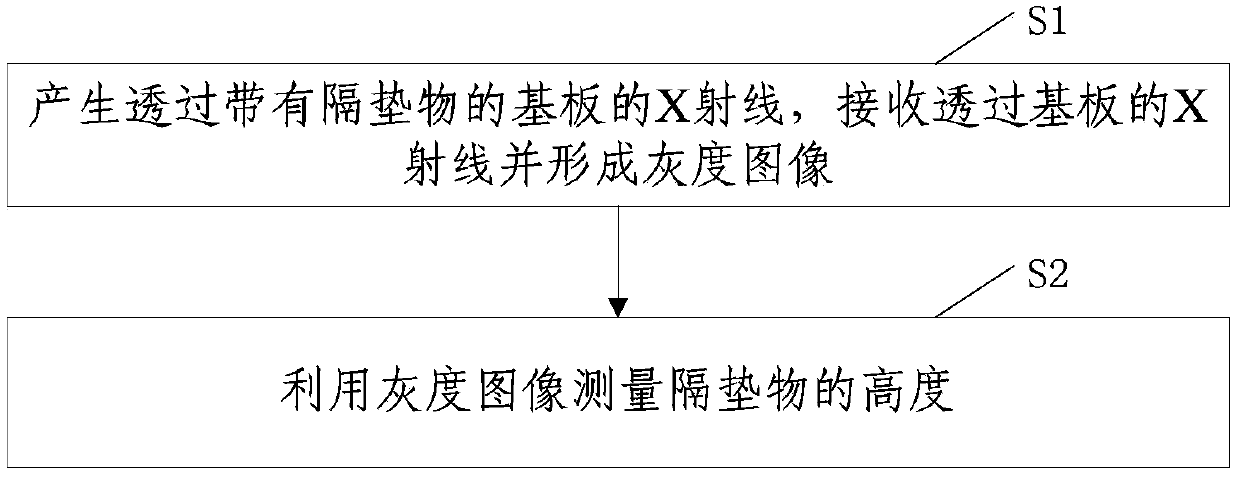
[0064] This embodiment provides a spacer detection method, such as Figure 4 As shown in the flow chart, including:
[0065] S1: Generate X-rays that pass through the substrate with a spacer, receive X-rays that pass through the substrate and form a grayscale image;
[0066] S2: Measuring the height of the spacer using the grayscale image.
[0067] In step S1, forming the grayscale image may be inversely compounding the reverse grayscale image and the front grayscale image of the same area to obtain a grayscale image for measuring the height of the spacer. For example, the reverse grayscale image and the front grayscale image of the same area can be obtained through the opposing X-ray imaging unit of the spacer detection device of the second embodiment, so that one of them can be reversed and composited with the other image. This eliminates artifacts caused by signal errors. In addition, if the gray value of a certain area of the gray image exceeds the set threshold, it m...
PUM
 Abstract
Description
Claims
Application Information
 - R&D
- Intellectual Property
- Life Sciences
- Materials
- Tech Scout
- Unparalleled Data Quality
- Higher Quality Content
- 60% Fewer Hallucinations
Browse by: Latest US Patents, China's latest patents, Technical Efficacy Thesaurus, Application Domain, Technology Topic, Popular Technical Reports.
© 2025 PatSnap. All rights reserved.Legal|Privacy policy|Modern Slavery Act Transparency Statement|Sitemap|About US| Contact US: help@patsnap.com