Overlay measurment device

a measurement device and overlay technology, applied in semiconductor/solid-state device testing/measurement, instruments, photomechanical equipment, etc., can solve problems such as difficult to accurately measure the height of the first overlay mark b>1/b>, and achieve the effect of accurately measuring the height and accurately measuring the overlay error

Pending Publication Date: 2022-10-13
AUROS TECH
View PDF0 Cites 0 Cited by
  • Summary
  • Abstract
  • Description
  • Claims
  • Application Information

AI Technical Summary

Benefits of technology

[0024]Since the overlay measurement device according to the present invention measures the height using light having a different wavelength for each layer, it is possible to accurately measure the height. Accordingly, it is possible to accurately measure an overlay error between layers having a large height difference and different optical properties.

Problems solved by technology

At this time, if the respective structures are not aligned within the error range permitted in the manufacturing processes, interference occurs between the electrically activated patterns.
This may cause problems in the performance and reliability of the manufactured circuit.
However, this method has a problem in that the heights of the first overlay mark 1 and the second overlay mark 2 are measured by an auto focus device using a single light source, without considering the fact that the first overlay mark 1 and the second overlay mark 2 are formed of different materials on different layers and the first overlay mark 1 is covered by a layer on which the second overlay mark 2 is formed.
Therefore, when the light source having a short wavelength is used, there is a problem in that it is difficult to accurately measure the height of the first overlay mark 1.
Conversely, when the light source having a long wavelength is used, there is a problem in that it is difficult to accurately measure the height of the second overlay mark 2.

Method used


Image

  • Overlay measurment device
  • Overlay measurment device
  • Overlay measurment device

Examples


Embodiment Construction

[0035]Hereinafter, exemplary embodiments of the present invention will be described in detail with reference to the accompanying drawings. However, the embodiments of the present invention may be modified into various other forms, and the scope of the present invention should not be construed as being limited to the embodiments described below. Embodiments of the present invention are provided to more completely describe the present invention to those of ordinary skill in the art. Accordingly, the shapes of elements in the drawings are exaggerated in order to emphasize a clearer description. The elements indicated by the same reference numerals in the drawings mean the same elements.

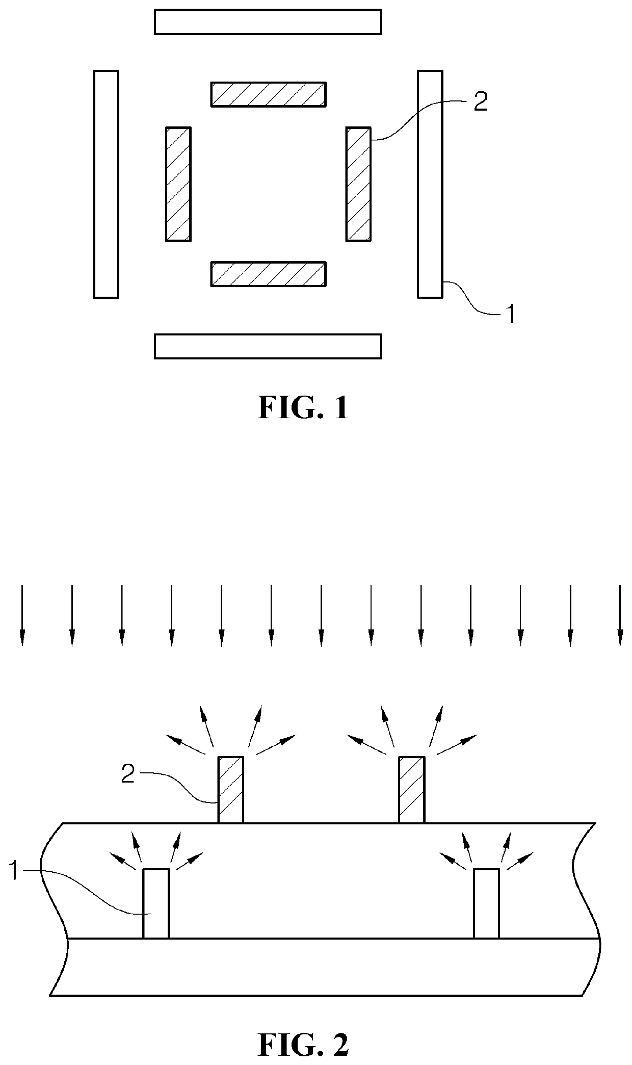
[0036]FIG. 6 is a conceptual diagram of an overlay measurement device according to an embodiment of the present invention. The overlay measurement device is a device that measures an error between a first overlay mark and a second overlay mark respectively formed on different layers formed on a wafer w.

[...


PUM

PropertyMeasurementUnit
angleaaaaaaaaaa
wavelengthaaaaaaaaaa
heightaaaaaaaaaa

Abstract

An overlay measurement device measures an error between a first overlay mark and a second overlay mark respectively formed on different layers formed on a wafer. The device is configured to detect a height of the first overlay mark based on a change in the signal of the first detector according to a change in the relative position of the objective lens with respect to the wafer in the optical axis direction and detect a height of the second overlay mark based on a change in the signal of the second detector according to a change in the relative position of the objective lens with respect to the wafer in the optical axis direction.

Description

TECHNICAL FIELD[0001]The present invention relates to an overlay measurement device. More particularly, the present invention relates to an overlay measurement device that includes an auto focus system using light sources of different wavelengths.BACKGROUND ART[0002]Along with technological development, a size of a semiconductor device is reduced, and an increase in the density of an integrated circuit is required. In order to satisfy these requirements, various conditions need to be satisfied. Among them, an overlay tolerance is one of important indicators.[0003]Semiconductor devices are manufactured through numerous manufacturing processes. In order to form an integrated circuit on a wafer, it is necessary to go through many manufacturing processes so that desired circuit structures and elements are sequentially formed at specific positions. The manufacturing processes allows patterned layers to be sequentially formed on the wafer. Through these repeated lamination processes, elec...

Claims


Application Information

Patent Timeline
Patent Type & Authority Applications(United States)
IPC IPC(8): G01B11/27G01B11/06G03F7/20G03F9/00
CPCG01B11/27G01B11/0608G03F7/70633G03F7/7085G03F9/7088H01L21/67259G01B11/02G03F7/20G01B2210/56G03F7/70575G03F7/70825H01L21/67242H01L22/30
Inventor PARK, GYU NAMSHIN, HYEON GILEE, SEUNG SOO
Owner AUROS TECH
Why Eureka
Try Eureka