Longitudinal super junction metal oxide field effect transistor

A technology of field effect transistors and oxides, which is applied to semiconductor devices, electrical components, circuits, etc., can solve problems such as uneven distribution of surface potential, drop of device withstand voltage, and aggregation of movable ions, so as to achieve uniform and stable surface potential distribution, Effects of improving reliability, improving pressure resistance and working stability

Active Publication Date: 2014-04-02
XIAN SEMIPOWER ELECTRONICS TECH
View PDF6 Cites 7 Cited by
  • Summary
  • Abstract
  • Description
  • Claims
  • Application Information

AI Technical Summary

Problems solved by technology

However, in the prior art, due to the uneven distribution of the surface potential of the terminal structure of the super-junction metal oxide effect transistor, the surface leakage phenomenon is prone to occur on the surface of the terminal withstand voltage structure, and at the same time, it will cause the aggregation of mobile ions, which makes the withstand voltage of the device decline

Method used


Image

  • Longitudinal super junction metal oxide field effect transistor
  • Longitudinal super junction metal oxide field effect transistor
  • Longitudinal super junction metal oxide field effect transistor

Examples


Embodiment Construction

[0026] The present invention will be further described in detail below in conjunction with specific embodiments, which are explanations of the present invention rather than limitations.

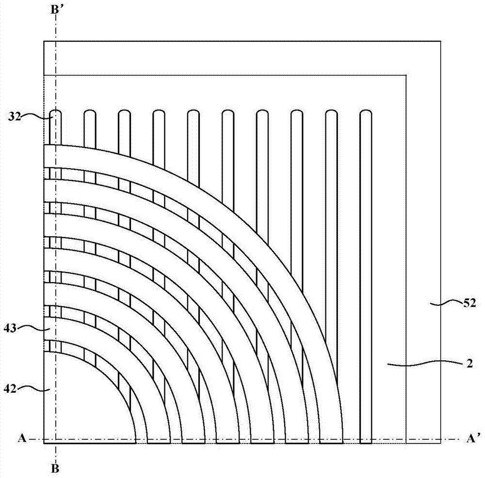
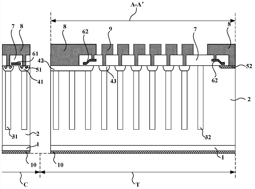
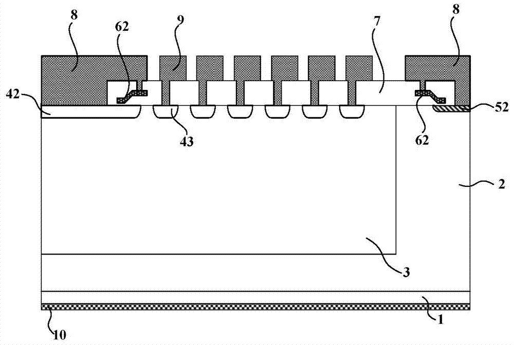
[0027] The vertical super junction metal oxide field effect transistor of the present invention, such as figure 2As shown, it includes an N-type doped semiconductor substrate 1 and an N-type doped epitaxial layer 2 sequentially arranged from bottom to top; the inside of the N-type doped epitaxial layer 2 is provided with a first P-type filling with the same structure from the inside to the outside. The well region 31 and the second P-type filled well region 32, the upper side of the first P-type filled well region 31 is provided with a first P-type doped region 41; the upper side of the second P-type filled well region 32 is from inside to outside A second P-type doped region 42 and a P-type doped equipotential ring 43 are provided, and the three together constitute the terminal withstand vo...


PUM


Abstract

The invention discloses a longitudinal super junction metal oxide field effect transistor, which comprises an N type doped semiconductor substrate and an N type doped epitaxial layer formed in sequence from bottom to top, wherein a first P type filling trap area and second P type filling trap areas with the same structures are formed inside the N type doped epitaxial layer from inside to outside; the upper side of the first P type filling trap area is provided with a first P type doped area; a second P type doped area and a P type doped unipotential ring are arranged on the upper side of each second P type filling trap area from inside to outside, and a terminal voltage-resistant structural area T is formed by the three parts; the second P type doped areas are arranged corresponding to the second P type filling trap areas; the P type doped unipotential rings are larger than the second P type filling trap areas in widths, and are correspondingly arranged in parallel over the second P type filling trap areas respectively along the length direction of the transistor; an N type doped area is arranged in each P type doped area, and constructs a primitive cell source electrode area C with the first P type filling trap area. By adopting the transistor, the surface potential distribution is optimized.

Description

technical field [0001] The invention belongs to the technical field of semiconductor power devices, and relates to a high-voltage power device, in particular to a vertical superjunction metal oxide field effect transistor. Background technique [0002] Traditional high-voltage power metal oxide semiconductor field effect transistor devices use a low-doped epitaxial drift layer as a voltage support layer, and its on-resistance is mainly the resistance of the drift layer. The withstand voltage capability of the drift layer is determined by its thickness and doping concentration. Therefore, in order to increase the breakdown voltage, it is necessary to increase the thickness of the drift layer and reduce its doping concentration at the same time. This causes the resistance of the drift layer to increase continuously. In the on state (especially at high voltage), the resistance of the drift layer accounts for most of the on resistance. [0003] The super junction metal oxide f...

Claims


Application Information

Patent Timeline
Patent Type & Authority Applications(China)
IPC IPC(8): H01L29/06H01L29/78H01L29/40
CPCH01L29/0619H01L29/063H01L29/402H01L29/404H01L29/78
Inventor 刘侠杨东林
Owner XIAN SEMIPOWER ELECTRONICS TECH
Why Eureka
Try Eureka