Plasma processing apparatus and method for adjusting process rate of marginal area of substrate

A processing device and plasma technology, applied to discharge tubes, electrical components, circuits, etc., can solve the problems of reduced yield, poor uniformity, and huge loss of edge effects of semiconductor process parts, so as to compensate for edge effects and avoid arcing The effect of discharge and ignition

Active Publication Date: 2014-04-09
ADVANCED MICRO FAB EQUIP INC CHINA
View PDF7 Cites 24 Cited by
  • Summary
  • Abstract
  • Description
  • Claims
  • Application Information

AI Technical Summary

Problems solved by technology

[0004] Since the semiconductor process part is circular, the area of ​​the outer ring is larger, and the poor uniformity of each process link in the edge part will lead to a significant drop in yield
Today, when the 300MHZ process is widely used, the loss caused by the edge effect of semiconductor process parts is even greater

Method used


Image

  • Plasma processing apparatus and method for adjusting process rate of marginal area of substrate
  • Plasma processing apparatus and method for adjusting process rate of marginal area of substrate
  • Plasma processing apparatus and method for adjusting process rate of marginal area of substrate

Examples


Embodiment Construction

[0059] The specific embodiments of the present invention will be described below in conjunction with the accompanying drawings.

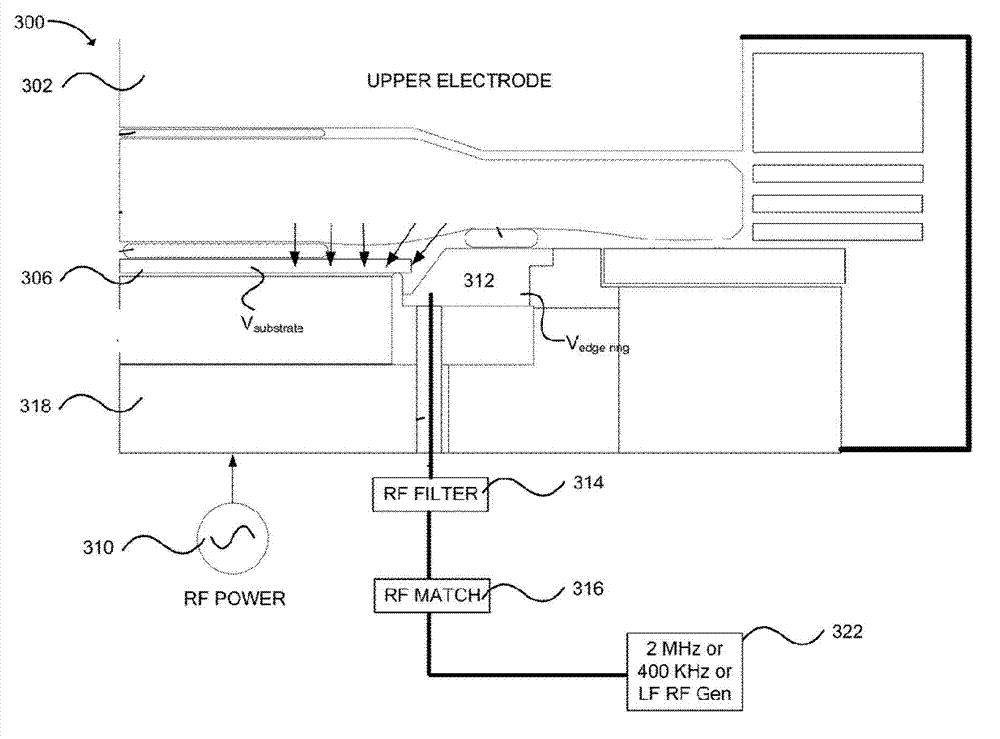
[0060] figure 1 It is a structural schematic diagram of a plasma processing device in the prior art, such as figure 1 As shown, the plasma processing apparatus 300 includes a parallel upper electrode 302 and a lower electrode 318, the lower electrode 318 is connected with a radio frequency power supply, and the substrate 306 is placed on the platform. A focus ring 312 is also provided on the periphery of the substrate 306 . The focus ring 312 is also connected to a low-frequency radio frequency power supply 322 , and a matching network 316 and a radio frequency filter 314 are connected in series between the low-frequency radio frequency power supply 322 and the focus ring 312 . In the prior art, the low-frequency radio frequency energy is coupled to the focus ring 312 near the periphery of the substrate 306 through the low-frequency filter 314 to ...


PUM


Abstract

The invention relates to a plasma processing apparatus and a method for adjusting a process rate of a marginal area of a substrate. The plasma processing apparatus comprises a cavity, a pedestal arranged in the cavity, a gas spay header arranged at the top of the cavity, a lower electrode arranged in the pedestal, a focusing ring arranged around the substrate, an edge electrode, and a phase shifter. To be specific, an electrostatic chuck is arranged above the pedestal; and a substrate is arranged above the electrostatic chuck. The gas spay header is used as an upper electrode; and process gas enters the cavity through the gas spay header. The lower electrode is connected with a first radio frequency power supply. The edge electrode approaches the edge area of the substrate and is connected with a second radio frequency power supply. And the phase shifter is connected with the first radio frequency power supply and the second radio frequency power supply. According to the invention, the edge effect can be effectively compensated; and phenomena of arc discharging and sparking due to the short distance between voltages applied to the central zone and the edge zone of the substrate can be avoided.

Description

technical field [0001] The invention relates to the field of semiconductor manufacturing, in particular to a plasma processing device and a method for adjusting the process rate in the edge region of a substrate. Background technique [0002] The plasma processing device uses the working principle of the vacuum reaction chamber to process the semiconductor substrate and the substrate of the plasma flat panel. The working principle of the vacuum reaction chamber is to pass a reaction gas containing an appropriate etchant or deposition source gas into the vacuum reaction chamber, and then input radio frequency energy to the vacuum reaction chamber to activate the reaction gas to ignite and maintain the plasma body, in order to respectively etch the material layer on the surface of the substrate or deposit the material layer on the surface of the substrate, and then process the semiconductor substrate and the plasma plate. For example, capacitive plasma reactors have been wide...

Claims


Application Information

Patent Timeline
Patent Type & Authority Applications(China)
IPC IPC(8): H01J37/32
Inventor 叶如彬尹志尧倪图强周宁
Owner ADVANCED MICRO FAB EQUIP INC CHINA
Why Eureka
Try Eureka