Method for preparing terminal structure by proton irradiation

A technology of proton irradiation and termination structure, applied in semiconductor/solid-state device manufacturing, electrical components, circuits, etc., can solve the problems of implantation damage and serious lateral diffusion of N-type wells, achieve small implantation damage, reduce chip terminal area, The effect of reducing leakage current

Active Publication Date: 2016-08-03
INST OF MICROELECTRONICS CHINESE ACAD OF SCI +2
View PDF5 Cites 0 Cited by
  • Summary
  • Abstract
  • Description
  • Claims
  • Application Information

AI Technical Summary

Problems solved by technology

High-temperature and long-time annealing will have a great impact on the process before forming the N-well and make the lateral diffusion of the N-type well very serious
The large implant energy required by the deep N-type well may exceed the existing process limit, and the large implant dose will cause more implant damage

Method used


Image

  • Method for preparing terminal structure by proton irradiation
  • Method for preparing terminal structure by proton irradiation
  • Method for preparing terminal structure by proton irradiation

Examples


Embodiment 1

[0043] A method for preparing a terminal structure by proton irradiation provided by an embodiment of the present invention includes the following steps:

[0044] Step SA1: preparing the main junction and P-type field limiting ring of the chip on the substrate;

[0045] Step SA2: preparing a meta-packet structure on the chip forming the main junction and the P-type field limiting ring;

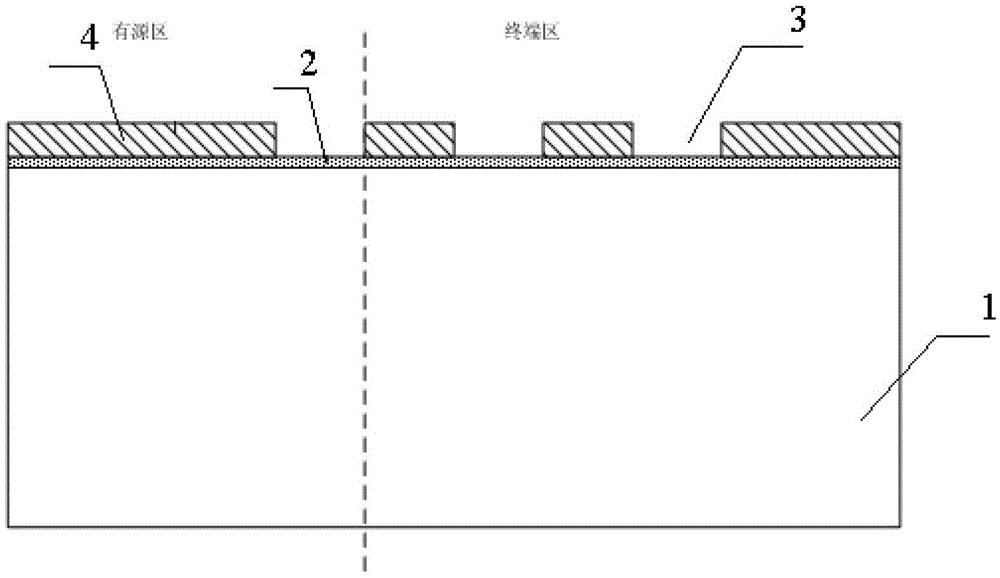
[0046] Step SA3: Combine Figure 8 As shown, after depositing metal electrodes on the chip forming the meta-packet structure, the cathode 18 is formed by etching;

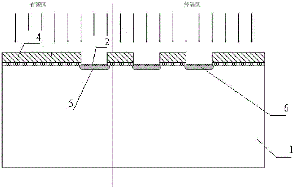
[0047] Step SA4: forming an N-type well by annealing after proton implantation on the chip where the cathode is formed, and completing the front-side process of the chip.

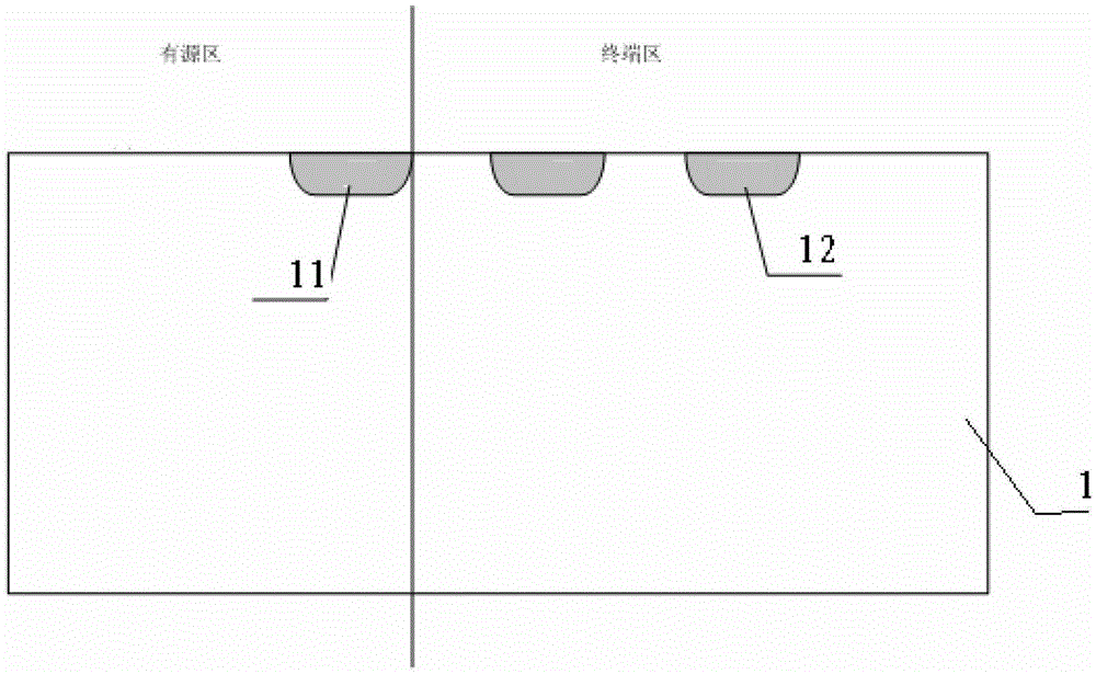
[0048] Step SA5: Combine Figure 11 As shown, after the P-type ion implantation is performed on the back of the chip that has completed the front-side process to form the P-collector 21, a metal electrode is deposited to form the anode 22, and the finished pr...

Embodiment 2

[0057] Step SB1: preparing the main junction and P-type field limiting ring of the chip on the substrate;

[0058] Step SB2: preparing a meta-packet structure on the chip forming the main junction and the P-type field limiting ring;

[0059] Step SB3: Combine Figure 8 As shown, after depositing metal electrodes on the chip forming the meta-packet structure, the cathode 18 is formed by etching;

[0060] Step SB4: forming an N-type well on the chip forming the cathode by annealing after proton implantation, and completing the front-side process of the chip;

[0061] Step SB5: Combine Figure 12 As shown, after the P-type ion implantation is performed on the back of the chip that has completed the front-side process to form the P-collector 21, a metal electrode is deposited to form the anode 22, and the finished product is obtained.

[0062] Wherein, step SA1 prepares the main junction and the P-type field limiting ring of the chip on the substrate including:

[0063] SB11: ...

Embodiment 3

[0070] The difference between this embodiment and Embodiment 1 is that the preparation of the main junction and P-type field limiting ring of the chip on the substrate in step SC2 includes:

[0071] Step SC21: After the oxide layer on the substrate is etched to obtain an oxide layer window, the substrate is first implanted with low-doped P-type impurities through the oxide layer window to form a low-doped P-type well at the main junction position and The low-doped P-type well in the terminal region is then implanted with highly doped P-type impurities to form a highly doped P-type well at the main junction position and a highly doped P-type well in the terminal region;

[0072] Step SC22: Remove the photoresist from the chip forming the highly doped P-type well at the main junction position and the highly doped P-type well at the terminal region, and perform heat treatment to form a low-doped P-type main junction and a highly doped P-type main junction. Junction, and low-doped...


PUM


Abstract

The invention discloses a method using proton irradiation to prepare a terminal structure. The method comprises the steps that a main junction and a P type field limiting ring of a chip are prepared on a substrate; an element package structure is prepared on the chip on which the main junction and the P type field limiting ring are formed; after metal electrode deposition is carried out on the chip on which the element package structure is formed, a cathode is formed through etching; after proton implantation is carried out on the chip on which the cathode is formed, an N type well is formed through annealing, and a front process of the chip is finished; and after P type ion implantation is carried out on the back of the chip whose front process is finished to form a P collector, metal electrode deposition is carried out to form an anode and a product is acquired. According to the method using proton irradiation to prepare the terminal structure, which is provided by the invention, voltage withstanding is ensured, and at the same time the chip terminal area is reduced; proton irradiation is used to form donor impurities, and the N type well is formed; the implantation damage is smaller compared with common high energy particle implantation; and the reliability of a device can be improved.

Description

technical field [0001] The invention relates to the field of power device preparation, in particular to a method for preparing a terminal structure by proton irradiation. Background technique [0002] An excellent terminal protection structure is an important guarantee for power devices (such as power diodes, power MOS tubes, IGBTs, etc.) to achieve a predetermined withstand voltage. On the basis of ensuring the withstand voltage, reducing the area of ​​the terminal area of ​​the device is an effective measure to reduce the cost of the device. The terminal structure that appeared earlier was the field limiting ring, and later there was a structure combining the field limiting ring and the field plate, and a terminal structure combined with terminal extension technology. [0003] In the traditional field-limiting ring structure, there are two ranges of field-limiting ring injection dose: 3e11-5e11cm 2 and 7e14-1e16cm 2 , all injected once. [0004] The traditional field-l...

Claims


Application Information

Patent Timeline
Patent Type & Authority Patents(China)
IPC IPC(8): H01L21/268H01L21/02
CPCH01L21/263H01L21/324
Inventor 褚为利朱阳军吴振兴赵佳
Owner INST OF MICROELECTRONICS CHINESE ACAD OF SCI
Why Eureka
Try Eureka