
A kind of igbt terminal structure and manufacturing method thereof

A terminal structure, N-type technology, used in semiconductor/solid-state device manufacturing, semiconductor devices, electrical components, etc., can solve problems such as large reverse leakage current and junction capacitance, complex thick insulating layer process, and low device current capacity. , to achieve the effect of reduced electric field strength, no increase in process steps, and improved efficiency and reliability

Active Publication Date: 2019-02-05
STATE GRID CORP OF CHINA +2
View PDF4 Cites 0 Cited by
  • Summary
  • Abstract
  • Description
  • Claims
  • Application Information

AI Technical Summary

Problems solved by technology

[0004] The terminal technologies currently used mainly include field-limiting ring technology, field plate technology, junction terminal extension technology, and lateral variable doping technology. Among them, the internationally renowned manufacturers use a four-step composite field plate structure (Infineon). The medium-thick insulating layer in the steps is complex and difficult to be compatible with the traditional process; the field-limited ring field plate structure (APT, Fuji Electric) has a large terminal size and low efficiency. Under the same chip area, the device has a small flow capacity; Terminal extension structure (ABB, Toshiba) and lateral variable doping structure (Infineon), both of which have relatively large reverse leakage current and junction capacitance, and are more sensitive to surface charges

Method used


Image

  • A kind of igbt terminal structure and manufacturing method thereof
  • A kind of igbt terminal structure and manufacturing method thereof
  • A kind of igbt terminal structure and manufacturing method thereof

Examples


Embodiment Construction

[0035] The specific implementation manners of the present invention will be further described in detail below in conjunction with the accompanying drawings.

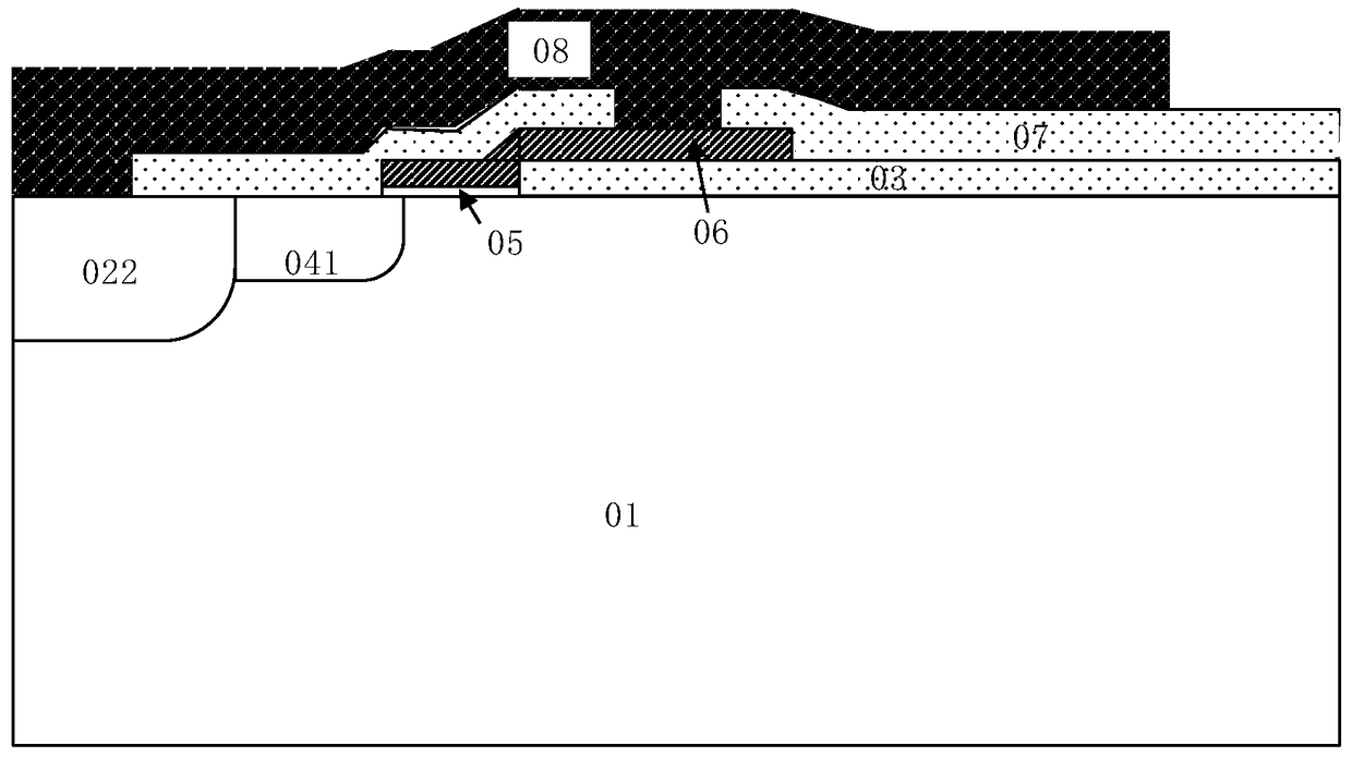
[0036] The schematic diagram of the IGBT terminal structure provided by the present invention is as figure 1 As shown, the IGBT terminal structure is connected to the IGBT active area, and the IGBT terminal structure includes N-type single crystal silicon chip 01, P-type field limiting ring 022, field oxide layer 03, gate oxide layer 05, polysilicon layer 06, boron phosphorus silicon Glass 07 and metal layer 08, the P-type field limiting ring 022 is located in the N-type single crystal silicon wafer 01, and the field oxide layer 03 and the gate oxide layer 05 are arranged in parallel, both located on the surface of the N-type single crystal silicon wafer 01 , the polysilicon layer 06 is located on the surface of the field oxide layer 03, the borophosphosilicate glass 07 is located on the surface of the field oxide layer ...


PUM


Abstract

The invention relates to an IGBT terminal structure and a manufacturing method thereof. The IGBT terminal structure comprises the components of an N-type monocrystalline silicon wafer, a P-type field limiting ring, a field oxide layer, a gate oxide layer, a polycrystalline silicon layer, boro-phospho-silicate-glass and a metal layer. The P-type field limiting ring is arranged in the N-type monocrystalline silicon wafer. The field oxide layer and the gate oxide layer are parallelly arranged and are respectively arranged on the surface of the N-type monocrystalline silicon wafer. The polycrystalline silicon layer is arranged on the surface of the field oxide layer. The boro-phospho-silicate-glass is arranged on the surface of the field oxide layer and extends to the surface of the polycrystalline silicon layer and the gate oxide layer. Metal connecting holes are etched on the boro-phospho-silicate-glass. The metal layer is connected with the P-type field limiting ring and the polycrystalline silicon layer through the metal connecting holes. A P-type ring with a junction depth which is smaller than that of the field limiting ring is added outside the P-type field limiting ring so that a depletion layer further expands when a PN junction deflects, thereby reducing electric field strength at a cylindrical surface junction position and realizing terminal efficiency improvement and reliability improvement. A same mask plate is used in the P-type ring which is added in the manufacturing method and P-well injection of an active region, and injection doping of the region is finished in P-well injection.

Description

technical field [0001] The invention relates to a semiconductor device, in particular to an IGBT terminal structure and a manufacturing method thereof. Background technique [0002] Due to the advantages of IGBT low switching loss, simple gate control, and excellent switch controllability, it is widely used in home appliance frequency conversion control, industrial control, locomotive transmission, power electronic devices, and new energy grid access. Since its invention in the 1980s, the vertical structure of the IGBT has experienced the development from the punch-through type, the non-punch-through type to the soft punch-through type, and the cell structure has experienced the development from the planar gate to the trench gate; the more power density the chip can handle It is getting bigger and bigger, but the loss is reduced instead, making it more and more obvious as a switching device in the high voltage field. [0003] In the IGBT manufacturing process, the diffusion...

Claims


Application Information

Patent Timeline
Patent Type & Authority Patents(China)
IPC IPC(8): H01L29/739H01L29/06H01L21/331
Inventor 王耀华赵哿李立
Owner STATE GRID CORP OF CHINA
Learn More