Semiconductor device and forming method thereof

一种半导体、器件的技术,应用在半导体制作工艺领域,能够解决降低横向双扩散MOS晶体管导通电阻、降低击穿电压、影响电路安全性等问题,达到击穿电压降低、提高导通电流、导通电阻降低的效果

Active Publication Date: 2015-03-25
SEMICON MFG INT (SHANGHAI) CORP
View PDF5 Cites 18 Cited by
  • Summary
  • Abstract
  • Description
  • Claims
  • Application Information

AI Technical Summary

Problems solved by technology

[0004] For the lateral double-diffused MOS transistor and the lateral insulated gate bipolar transistor, on-resistance and breakdown voltage are the two most important electrical parameters, wherein the on-resistance is inversely proportional to the doping concentration of the drift region, and the breakdown voltage is inversely proportional to the doping concentration of the drift region. The doping concentration of the drift region is inversely proportional, although the higher doping concentration of the drift region is beneficial to reduce the on-resistance of the lateral double-diffused MOS transistor and the lateral insulated gate bipolar transistor, and improve the lateral double-diffused MOS transistor and the lateral insulated gate bipolar transistor. The conduction current of the pole transistor, but it will reduce the breakdown voltage and affect the safety of the circuit

Method used


Image

  • Semiconductor device and forming method thereof
  • Semiconductor device and forming method thereof
  • Semiconductor device and forming method thereof

Examples


Embodiment Construction

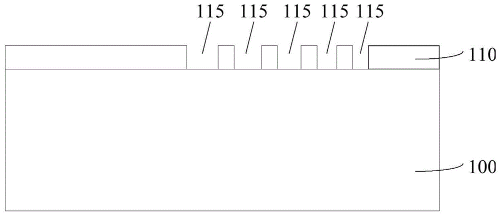
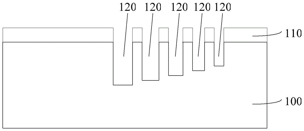
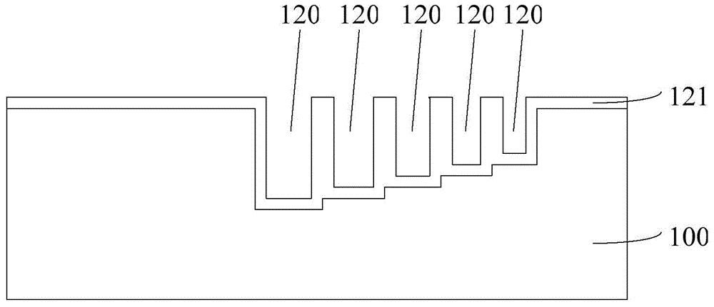
[0024] In the existing lateral double-diffused MOS transistors or lateral insulated gate bipolar transistors, although the higher doping concentration of the drift region is conducive to improving the conduction current of the lateral double-diffused MOS transistors or lateral insulated gate bipolar transistors, it will lower breakdown voltage. And when the doping concentration of the drift region is low, the surface electric field of the drain junction is high, and breakdown first occurs at the position where the drain region and the drift region are in contact. When the doping concentration of the drift region is high, the drift region is close to the body region It becomes easy to break down between the semiconductor substrates.

[0025] Therefore, the present invention provides a semiconductor device and a forming method thereof, the semiconductor device is a lateral double-diffused MOS transistor or a lateral insulated gate bipolar transistor, specifically comprising: a s...


PUM


Abstract

A semiconductor device and a forming method thereof are provided. The semiconductor device comprises a semiconductor substrate, a body region and a drift region disposed in the semiconductor substrate, a body connecting region and a source region disposed in the body region, a drain region and a first shallow trench isolation structure disposed in the drift region, and a gate structure disposed on the surface of the semiconductor substrate and across the edges of the body region and the drift region, wherein the first shallow trench isolation structure is disposed between the drain region and the body region, the bottom of the first shallow trench isolation structure is step-shaped, the adjacent steps are not the same in depth, and the gate structure covers part of the surface of the first shallow trench isolation structure. The on resistance of the drift region can be reduced and the on current of the drift region can be increased without lowering the voltage endurance capability.

Description

technical field [0001] The invention relates to a semiconductor manufacturing process, in particular to a semiconductor device and a forming method. Background technique [0002] At present, lateral double diffused MOS transistors (LDMOS, Lateral Double diffused MOSFET) and lateral insulated gate bipolar transistors (LIGBT, Lateral Insulated Gate Bipolar Transistor) are widely used in analog power management, chargers, DC-DC converters, AC- in the DC converter circuit. And as the feature size of the CMOS process keeps shrinking, in order to improve the work efficiency and reduce the area of ​​the chip, it is necessary for the lateral double-diffused MOS transistor and the lateral insulated gate bipolar transistor to have as small an on-resistance (Ron) as possible. [0003] At the same time, due to the continuous shrinking of the feature size of CMOS technology, the ability of transistors to withstand high voltage and high current is continuously reduced, and deep submicron...

Claims


Application Information

Patent Timeline
Patent Type & Authority Applications(China)
IPC IPC(8): H01L21/336H01L21/331H01L29/78H01L29/739
CPCH01L21/76229H01L29/66659H01L29/7835H01L29/0653H01L29/1045H01L29/7816H01L29/7393H01L29/66325H01L29/66681
Inventor 杨广立俞谦荣汪铭蒲贤勇
Owner SEMICON MFG INT (SHANGHAI) CORP
Why Eureka
Try Eureka