Ultralow forward-voltage-drop Trench Schottky device and manufacturing method

A forward voltage drop, device technology, applied in semiconductor/solid state device manufacturing, semiconductor devices, electrical components, etc., can solve the problems of reducing forward voltage drop, low temperature change, etc., to reduce forward voltage drop, terminal length, etc. The effect of reducing and increasing the effective cell area

Inactive Publication Date: 2018-09-04
JIANGSU JIEJIE MICROELECTRONICS
View PDF4 Cites 0 Cited by
  • Summary
  • Abstract
  • Description
  • Claims
  • Application Information

AI Technical Summary

Problems solved by technology

[0002] In the field of power semiconductor devices, traditional Schottky diodes use metal-semiconductor Schottky contacts to achieve better rectification characteristics, but to meet the withstand voltage requirements of medium and high voltage devices, traditional Schottky diodes are The base barrier is low and changes greatly with temperature, so it is no longer widely applicable. In recent years, another type of Schottky diode device has appeared. They use Trench trench structure and grow a certain thickness of insulating oxide layer on the inner wall of the trench. , and fill the trench with conductive polysilicon, so that the conductive polysilicon, the insulating oxide layer, and the semiconductor substrate material form a capacitive plate structure. When the device needs to withstand voltage, the semiconductor substrate applies a high potential relative to the conductive polysilicon. The charge opposite to the doping type of the semiconductor is coupled from the substrate near the trench, and a depletion layer is further formed under the action of the reverse bias voltage. Before the two adjacent depletion layers are in contact, the voltage applied on the semiconductor substrate is controlled by the device The Schottky barrier formed by the anode metal and the semiconductor substrate is borne, and by controlling the distance between adjacent trenches, the thickness of the insulating oxide layer in the trench, and the resistivity of the semiconductor substrate, the adjacent depletion layer can be determined. It can be contacted under high voltage. Once the depletion layer contacts are connected together, the voltage of the semiconductor substrate will be borne by the depletion layer. Therefore, the Trench Schottky diode has a high reverse breakdown voltage. The Schottky diode can also reduce the forward voltage drop without changing the reverse breakdown voltage

Method used


Image

  • Ultralow forward-voltage-drop Trench Schottky device and manufacturing method
  • Ultralow forward-voltage-drop Trench Schottky device and manufacturing method
  • Ultralow forward-voltage-drop Trench Schottky device and manufacturing method

Examples


Embodiment Construction

[0042] The present invention will be further described below in conjunction with specific drawings and embodiments.

[0043] The present invention is not limited to the following embodiments, and the figures referred to in the following descriptions are provided for understanding the content of the present invention, that is, the present invention is not limited to the device structures illustrated in the figures.

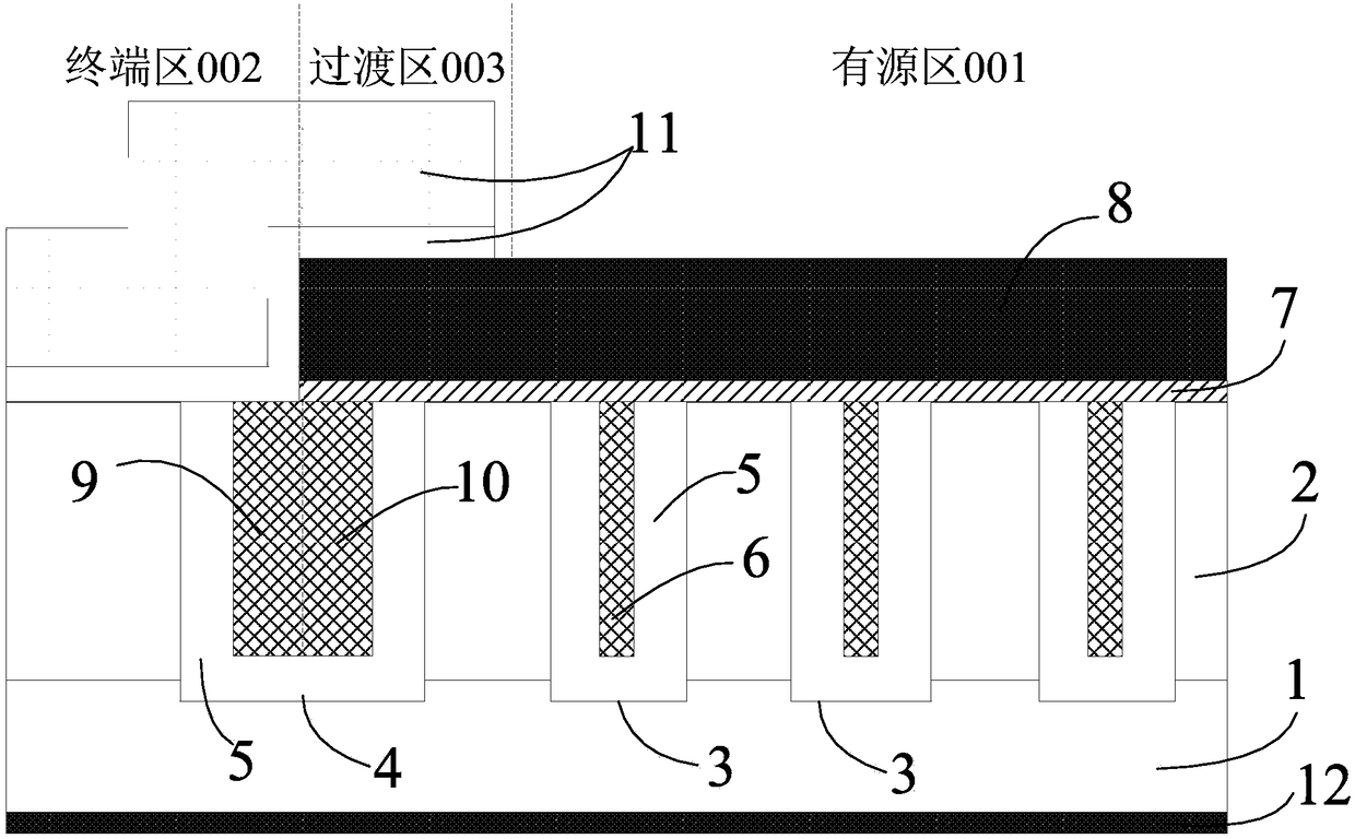
[0044] Such as figure 1As shown, Embodiment 1 takes a 100V Trench Schottky device as an example, a Trench Schottky device with an ultra-low forward voltage drop, including an active region 001 and a terminal region 002 located on a semiconductor substrate, in the Schottky On the top view plane of the base device, the active region 001 is located in the central region of the semiconductor substrate, and the terminal region 002 is located at the outer ring of the active region 001 and surrounds the active region 001; in the cross-section of the Schottky device Above...


PUM


Abstract

The invention belongs to the technical field of the manufacturing of semiconductor devices and relates to an ultralow forward-voltage-drop Trench Schottky device. A semiconductor base plate comprisesa drift region and a substrate which are respectively located at the upper and lower parts of the semiconductor base plate, wherein the substrate is adjacent to the drift region, a first main surfaceof the semiconductor base plate is formed on the upper surface of the drift region, and a second main surface of the semiconductor base plate is formed on the lower surface of the substrate; a plurality of uniformly distributed grooves are formed in the semiconductor base plate in an active region, penetrate through the drift region in the direction from the first main surface to the second main surface and extend into the substrate; a wide groove is formed in the semiconductor base plate in a transition region and a terminal region close to the transition region and penetrates through the drift region in the direction from the first main surface to the second main surface and extends into the substrate; and a passivation layer is settled on the first main surface of the semiconductor baseplate in the terminal region. By utilizing a relative deep groove structure, the device has relatively low forward voltage drop, so that the forward conduction power dissipation is reduced, and the cost is lowered.

Description

technical field [0001] The invention relates to a Schottky device and a manufacturing method, in particular to an ultra-low forward voltage drop Trench Schottky device and a manufacturing method, and belongs to the technical field of manufacturing semiconductor devices. Background technique [0002] In the field of power semiconductor devices, traditional Schottky diodes use metal-semiconductor Schottky contacts to achieve better rectification characteristics, but to meet the withstand voltage requirements of medium and high voltage devices, traditional Schottky diodes are The base barrier is low and changes greatly with temperature, so it is no longer widely applicable. In recent years, another type of Schottky diode device has appeared. They use Trench trench structure and grow a certain thickness of insulating oxide layer on the inner wall of the trench. , and fill the trench with conductive polysilicon, so that the conductive polysilicon, the insulating oxide layer, and ...

Claims


Application Information

Patent Timeline
Patent Type & Authority Applications(China)
IPC IPC(8): H01L29/872H01L21/329
CPCH01L29/66143H01L29/872
Inventor 刘锋周祥瑞殷允超
Owner JIANGSU JIEJIE MICROELECTRONICS
Why Eureka
Try Eureka