Flexible circuit board and chip package structure

A flexible circuit board and chip technology, applied in circuits, printed circuit components, electrical components, etc., can solve the problems of large impact on circuit board quality, poor pad rigidity, failure, etc.

Active Publication Date: 2014-04-09
AVARY HLDG (SHENZHEN) CO LTD +1
View PDF6 Cites 4 Cited by
  • Summary
  • Abstract
  • Description
  • Claims
  • Application Information

AI Technical Summary

Problems solved by technology

Among them, the performance of the circuit board has a great influence on the quality of the le

Method used


Image

  • Flexible circuit board and chip package structure
  • Flexible circuit board and chip package structure
  • Flexible circuit board and chip package structure

Examples


Embodiment Construction

[0017] The flexible circuit board and chip packaging structure provided by the technical solution will be further described in detail below in conjunction with the accompanying drawings and four embodiments.

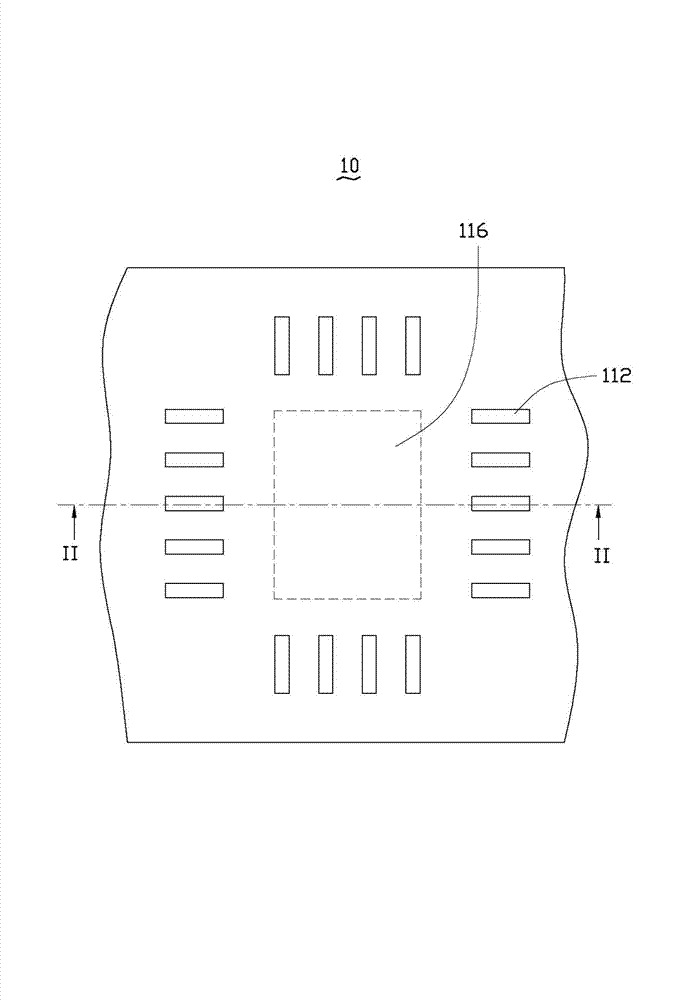
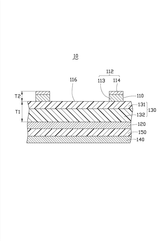
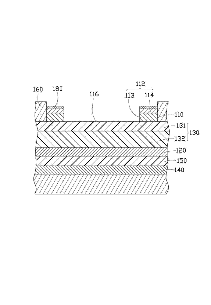
[0018] see figure 1 and figure 2 , the first embodiment of the technical solution provides a flexible circuit board 10, the flexible circuit board 10 includes a first conductive layer 110, a first insulating layer 130, a second conductive layer 120, a second insulating layer 150 and a third conductive Layer 140.

[0019] The first conductive layer 110 includes at least one conductive circuit pattern (not shown in the figure) and a plurality of welding pads 112 . The plurality of pads 112 are used to electrically connect with the semiconductor chip through wires. The area surrounded by the plurality of bonding pads 112 forms a chip bonding area 116 , and the chip bonding area 116 is used for bonding chips. In this embodiment, the die bonding area 116 is a part of the...


PUM

PropertyMeasurementUnit
Thicknessaaaaaaaaaa
Thicknessaaaaaaaaaa
Thicknessaaaaaaaaaa

Abstract

The invention relates to a flexible circuit board which is used for chip package and a chip package structure. The provided flexible circuit board comprises a first conductive layer, a second conductive layer and a first insulation layer. The first insulation layer is located between the first conductive layer and the second conductive layer. The first conductive layer comprises a number of pads. A number of pads are electrically connected with a chip through leads. A region surrounded by a number of pads forms a chip bonding region. The chip bonding region is used for chip bonding. The thickness of each pad is defined to be T1, and the thickness of the first insulation layer is defined to be T2, wherein 63 microns<=(T1+T2)<=87 microns, and 0.44<= (T1/T2) <=0.64.

Description

technical field [0001] The invention relates to the field of chip packaging, in particular to a flexible circuit board and a chip packaging structure that can be used for chip packaging. Background technique [0002] Generally, the packaging method of a semiconductor chip is: a plurality of welding pads are arranged on the circuit board, and the plurality of welding pads are external electrical connection points of the semiconductor chip; a semiconductor chip is provided, and several welding pads are provided on the semiconductor chip. Electrical contact pads; respectively weld the electrical contact pads on the semiconductor chip and the pads on the circuit board through several bonding wires, so that the semiconductor chip and the circuit board are electrically connected, that is, through wire bonding A semiconductor chip is placed on a circuit board. Among them, the performance of the circuit board has a great influence on the quality of the lead welding, for example, po...

Claims


Application Information

Patent Timeline
IPC IPC(8): H01L23/498H01L23/31H05K1/02
CPCH01L2224/48091H01L2224/73265H01L2924/00014
Inventor 何四红
Owner AVARY HLDG (SHENZHEN) CO LTD
Why Eureka
Try Eureka