Array substrate drive circuit, array substrate and corresponding liquid crystal displayer

A technology for liquid crystal displays and array substrates, applied in static indicators, instruments, nonlinear optics, etc., can solve the problems of unfavorable narrow-frame design, complex circuits, and large occupied area of ​​the GoA drive unit, and is conducive to narrow-frame design. , the effect of reducing complex procedures and reducing area

Active Publication Date: 2014-04-16
TCL CHINA STAR OPTOELECTRONICS TECH CO LTD
View PDF7 Cites 51 Cited by
  • Summary
  • Abstract
  • Description
  • Claims
  • Application Information

AI Technical Summary

Problems solved by technology

[0004] like figure 1 As shown, it shows a schematic structural diagram of an array substrate driving circuit using unilateral drive in the prior art; in this kind of unilaterally driven array substrate, each row corresponds to a GoA drive unit, and usually 7 GoA drive units are used. For the above TFT transistors, for the panel side of the GoA circuit, the frame design will be wider, which is not conducive to the narrow frame design
[0005] like figure 2 As shown, it shows a structural schematic diagram of an array substrate driving circuit using double-sided driving in the prior art; in this kind of double-sided driven array substrate, it has a symmetrical structure, and each row uses two GoA drive units for double-sided driving. The advantage of this design is to improve the gate drive capability, but the disadvantage is that the circuit is complex, and the GoA drive unit occupies a large area, which is not conducive to narrow frame design

Method used


Image

  • Array substrate drive circuit, array substrate and corresponding liquid crystal displayer
  • Array substrate drive circuit, array substrate and corresponding liquid crystal displayer
  • Array substrate drive circuit, array substrate and corresponding liquid crystal displayer

Examples


Embodiment Construction

[0040] The following descriptions of the various embodiments refer to the accompanying drawings to illustrate specific embodiments in which the present invention can be implemented. The directional terms mentioned in the present invention, such as "up", "down", "front", "back", "left", "right", "inside", "outside", "side", etc., are for reference only The orientation of the attached schema. Therefore, the directional terms used are used to illustrate and understand the present invention, but not to limit the present invention.

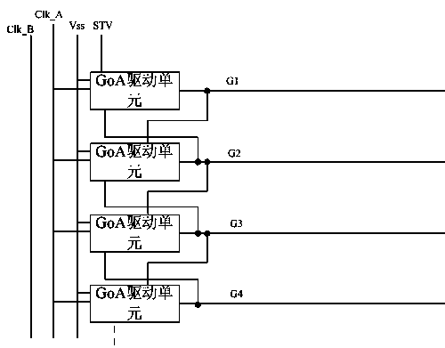
[0041] Such as image 3 Shown is a schematic structural diagram of an embodiment of the array substrate driving circuit of the present invention; in this embodiment, the array substrate driving circuit includes a plurality of GoA driving units for driving the gate lines of the array substrate, wherein each The GoA drive unit is connected to a gate line;

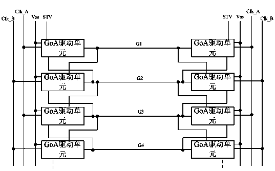
[0042] The GoA driving units connected to the gate lines of odd rows are arranged on one side o...


PUM


Abstract

The embodiment of the invention discloses an array substrate drive circuit which comprises a plurality of GoA drive units. Each GoA drive unit is connected with a grid line; the GoA drive units connected with the grid lines in odd-number lines are arranged at one side of an array substrate and the GoA drive units connected with the grid lines in even-number lines are arranged at the other side of the array substrate; each GoA drive unit is provided with two drive signal input ends and one input end, every two drive signal input ends are connected with the output end of the upper-level GoA drive unit and the output end of the lower-level GoA drive unit respectively and used for receiving drive signals output by the upper-level GoA drive unit and the lower-level GoA drive unit, drive signals of the GoA drive unit of the level is output to one grid line connected with the GoA drive unit through the output end, and the GoA drive units arranged at the two sides of the array substrate drive the grid lines of the array substrate in an alternating mode. The embodiment of the invention further discloses the array substrate and a liquid crystal displayer. According to the array substrate drive circuit, the array substrate and the liquid crystal displayer, area occupied by the array substrate drive circuit can be reduced and narrow frame design of the liquid crystal displayer is facilitated.

Description

technical field [0001] The present invention relates to the field of thin film transistor liquid crystal display (Thin Film Transistor liquid crystal display, TFT-LCD), in particular to an array substrate driving circuit, an array substrate and a corresponding liquid crystal display. Background technique [0002] Liquid crystal display technology has developed rapidly, and great progress has been made in terms of screen size and display quality. Liquid crystal display has the characteristics of small size, low power consumption, and no radiation, and has now occupied a dominant position in the field of flat-panel display. . With the development of liquid crystal display technology, high resolution, high contrast, high refresh rate, narrow frame, and thinning have become the development trend of liquid crystal display; [0003] At present, TFT (Thin Film Transistor, thin film transistor) is often used to set up GoA (Gate On Array, array gate drive) circuit. In order to reali...

Claims


Application Information

Patent Timeline
Patent Type & Authority Applications(China)
IPC IPC(8): G09G3/36G02F1/1362G02F1/1368G02F1/133
CPCG09G2300/0408G09G2300/0426G09G2310/0286G09G3/3674G09G3/36G09G3/3648G09G3/3659G09G2310/0272G09G2320/0223
Inventor 徐向阳
Owner TCL CHINA STAR OPTOELECTRONICS TECH CO LTD
Why Eureka
Try Eureka