Method of manufacturing a photovoltaic silicon
A manufacturing method and optoelectronic technology, applied in chemical instruments and methods, semiconductor/solid-state device manufacturing, circuits, etc., can solve problems such as low production efficiency and achieve the effect of reducing manufacturing costs
- Summary
- Abstract
- Description
- Claims
- Application Information
AI Technical Summary
Problems solved by technology
Method used
Image
Examples
Embodiment 1
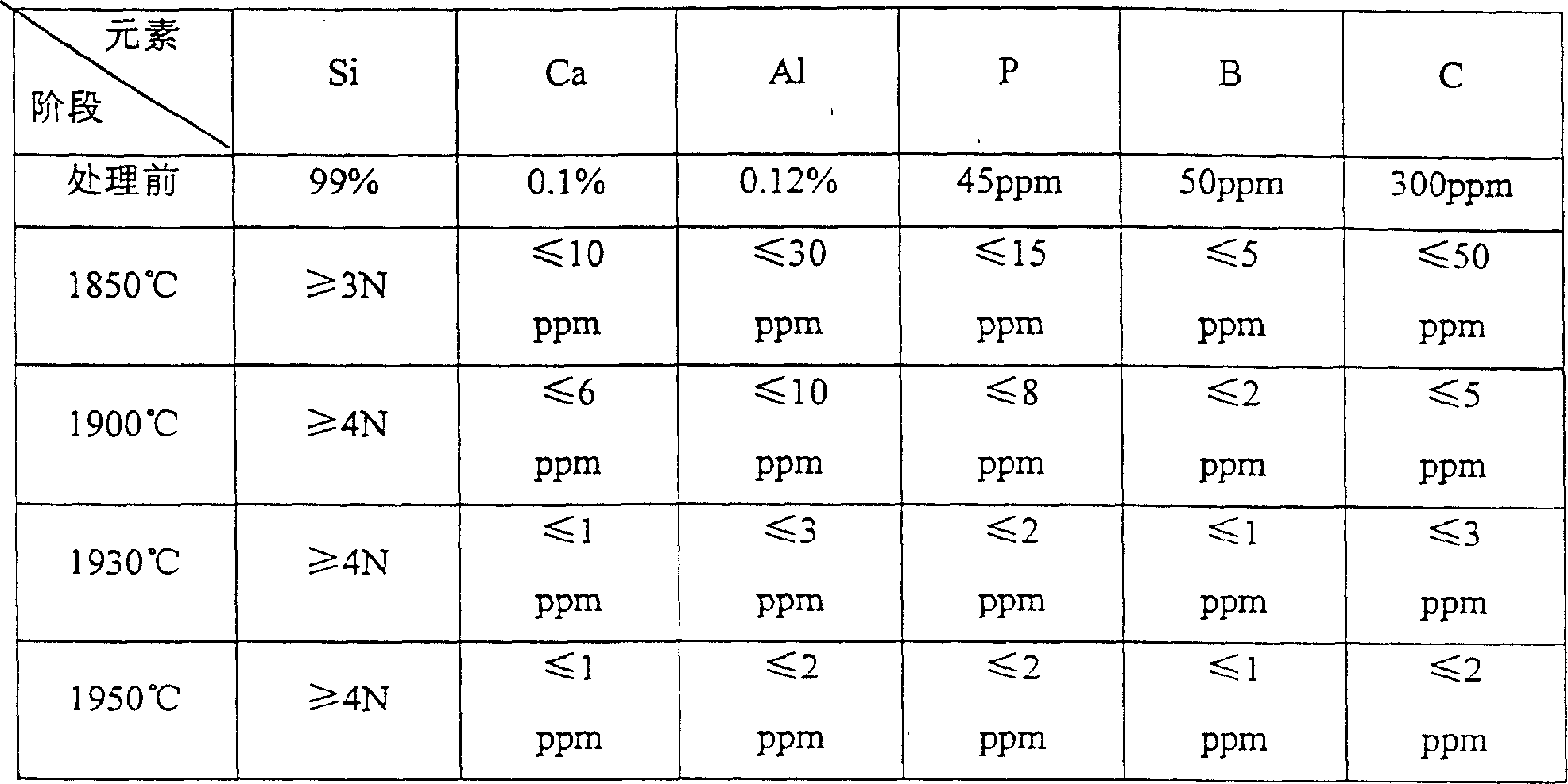
[0015] In the vacuum negative pressure chamber, use an intermediate frequency induction furnace to raise the temperature to 1850°C, melt the raw material chemical grade silicon, remove aluminum, boron, phosphorus, sulfur, carbon, etc.; under the protection of nitrogen, pass 1:1.4 into the silicon melt Water vapor and hydrogen, the amount of gas introduced can be 16Kg / min, stirred and refined for 4 hours, other elements are vaporized at high temperature and then poured into the coagulator; directional solidification is carried out from bottom to top in the vacuum negative pressure chamber to remove iron and other Heavy metals; slowly cool down to room temperature to obtain photoelectric grade silicon. A water jacket is used at the bottom of the coagulator to control the flow rate of water to achieve the purpose of slow cooling, so as to control its coagulation speed.
Embodiment 2
[0017] In the vacuum negative pressure chamber, use an intermediate frequency induction furnace to raise the temperature to 1900°C, melt the chemical grade silicon as the raw material, and remove aluminum, boron, phosphorus, sulfur, carbon, etc.; under the protection of argon, pass 1:1.5 Stir and refine for 3 hours to vaporize other elements at high temperature and pour them into the coagulator; carry out directional solidification from bottom to top in the vacuum negative pressure chamber to remove iron and other heavy metals; slowly cool down to room temperature to obtain photoelectricity grade silicon.
Embodiment 3
[0019] In the vacuum negative pressure chamber, use an intermediate frequency induction furnace to raise the temperature to 1930°C, melt the chemical grade silicon as raw material, and remove aluminum, boron, phosphorus, sulfur, carbon, etc.; Water vapor and hydrogen are stirred and refined for 3.5 hours, and other elements are vaporized at high temperature and then poured into a coagulator; directional solidification is carried out from bottom to top in a vacuum negative pressure chamber to remove iron and other heavy metals; the temperature is slowly cooled to room temperature to obtain a photoelectric grade silicon.
PUM
| Property | Measurement | Unit |
|---|---|---|
| melting point | aaaaa | aaaaa |
Abstract
Description
Claims
Application Information
 - R&D
- Intellectual Property
- Life Sciences
- Materials
- Tech Scout
- Unparalleled Data Quality
- Higher Quality Content
- 60% Fewer Hallucinations
Browse by: Latest US Patents, China's latest patents, Technical Efficacy Thesaurus, Application Domain, Technology Topic, Popular Technical Reports.
© 2025 PatSnap. All rights reserved.Legal|Privacy policy|Modern Slavery Act Transparency Statement|Sitemap|About US| Contact US: help@patsnap.com

