Reverse-side printing process for resistor protruding electrode

A technology of reverse printing and resistors, applied in resistors, resistor manufacturing, circuits, etc., can solve the problems of low TCR level of products, bruised electrodes at the resistor terminals, and easy dispersion of the initial value of the resistor, so as to avoid the function failure of the original resistor, The effect of improving the TCR level and shortening the current stroke

Active Publication Date: 2014-04-16
RALEC TECH KUNSHAN LTD
View PDF4 Cites 6 Cited by
  • Summary
  • Abstract
  • Description
  • Claims
  • Application Information

AI Technical Summary

Problems solved by technology

However, the above-mentioned chip resistor manufacturing method has the following disadvantages: 1. Since the front electrode is made of silver paddle material, and the front electrode is realized by screen printing, the thickness of the film layer is likely to be uneven. After the resistance layer is printed, the initial value of the resistance is easy to disperse. Leading to increased difficulty in production control and increased non-compliance
2. The printed silver paste material is used to form the front electrode of the chip resistor. After firing, the thickness is thicker and the amount used is larger, and the printed material is a sintered paste with silver as the main component. Its price is relatively high, resulting in product The production cost is high and the market competitiveness is weakened
However, the following problems will arise: In the process of testing the product, when the customer loads the resistor into the test equipment, for the convenience of testing, the plug-in method is often used.
Due to the plug-in method, during the plug-in process, the terminal electrode of the resistor is directly in contact with the test equipment, and due to the manual operation test, it is easy to cause damage to the resistor terminal electrode, which will lead to the failure of the original resistor function and the low TCR level of the product.

Method used


Image

  • Reverse-side printing process for resistor protruding electrode
  • Reverse-side printing process for resistor protruding electrode
  • Reverse-side printing process for resistor protruding electrode

Examples


Embodiment 1

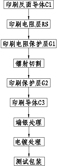
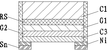
[0052] In this embodiment, the thickness of the reverse conductor C1 is 150 μm, and the ink printing temperature of the reverse conductor C1 is 850°C. The thickness of the resistance layer RS ​​is 15 μm, the ink printing temperature of the resistance layer RS ​​is 850° C., and the resistance value range of the resistance layer RS ​​is ±35% of the required resistance value. The thickness of the resistance protection layer G1 was 15 μm, and the ink printing temperature of the resistance protection layer G1 was 600°C. The thickness of the protective layer G2 was 15 μm, and the ink printing temperature of the protective layer G2 was 190°C. The thickness of the conductor C3 is 150 μm, and the ink printing temperature of the conductor C3 is 230°C.

Embodiment 2

[0054] In this embodiment, the thickness of the reverse conductor C1 is 15 μm, and the ink printing temperature of the reverse conductor C1 is 800°C. The thickness of the resistance layer RS ​​is 5 μm, the ink printing temperature of the resistance layer RS ​​is 800° C., and the resistance value range of the resistance layer RS ​​is ±35% of the required resistance value. The thickness of the resistance protection layer G1 was 5 μm, and the ink printing temperature of the resistance protection layer G1 was 550°C. The thickness of the protective layer G2 is 5, and the ink printing temperature of the protective layer G2 is 140°C. The thickness of the conductor C3 is 15 μm, and the ink printing temperature of the conductor C3 is 180°C.

Embodiment 3

[0056] In this embodiment, the thickness of the reverse conductor C1 is 300 μm, and the ink printing temperature of the reverse conductor C1 is 900°C. The thickness of the resistance layer RS ​​is 25 μm, the ink printing temperature of the resistance layer RS ​​is 900° C., and the resistance value range of the resistance layer RS ​​is ±35% of the required resistance value. The thickness of the resistance protection layer G1 was 25 μm, and the ink printing temperature of the resistance protection layer G1 was 650°C. The thickness of the protective layer G2 was 25 μm, and the ink printing temperature of the protective layer G2 was 240°C. The thickness of the conductor C3 is 300 μm, and the ink printing temperature of the conductor C3 is 280°C.


PUM


Abstract

The invention discloses a reverse-side printing process for a resistor protruding electrode. The process comprises the following steps: (1) printing a reverse-side conductor; (2) printing a resistor layer; (3) printing a resistor protective layer; (4) performing laser cutting; (5) printing a protective layer; (6) printing a conductor; (7) performing terminated sliver treatment; (8) performing electroplating treatment; and (9) testing and packaging. By adoption of the technical scheme, the reverse-side printing process has the beneficial effects that a phenomenon that an original resistor function is ineffective when a user impacts a terminal electrode during use is effectively avoided, the resistor printing side faces downwards in the process of arranging the parts by a client, the current stroke is shortened, the TCR level of the product is improved, and the cost is reduced.

Description

technical field [0001] The invention relates to a resistor printing process, in particular to a reverse printing process of a protruding electrode of a resistor. Background technique [0002] In the prior art, resistors are widely used in electronic circuits. The manufacturing method of a typical chip resistor is as follows: 1. Use screen printing to form the front electrode on the front of a large insulating substrate, and dry it; 2. Use screen printing to form the back electrode on the back of the above insulating substrate, and perform Dry and fire; 3. Use screen printing to form a resistance layer on the inside of the above-mentioned front electrode, dry and fire, and the two ends of the resistance layer are connected to the above-mentioned front electrode; 4. Form the first resistance layer on the above-mentioned resistance layer. A protective layer (i.e. glass protective layer), and drying and firing; 5. For the above-mentioned resistance layer, the resistance is prec...

Claims


Application Information

Patent Timeline
Patent Type & Authority Applications(China)
IPC IPC(8): H01C17/00
Inventor 管春风
Owner RALEC TECH KUNSHAN LTD
Why Eureka
Try Eureka